Sixty Years of Memory Scaling, 1966–2026: Why Arithmetic Became Almost Free and Moving a Bit Did Not
A technical report. Draft for publication, September 2026.
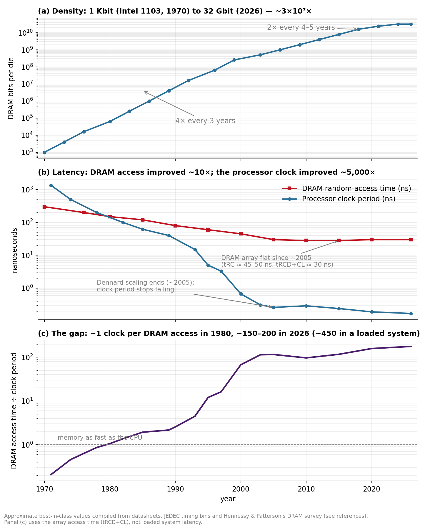
Reading guide. Part I states the problem in one page and checks the standard explanation. Part II is the sixty-year history, era by era. Parts III–VI go deep on the four "walls" that compound into the memory wall: the DRAM cell, the on-chip wire, the off-chip link, and the memory-system organization. Part VII covers the architectural response (caches everywhere), Part VIII the compute side of the divergence, and Part IX projections through 2040. Appendices contain derivations and data tables. All numbers are order-of-magnitude engineering figures unless a source is named; the references section identifies which figures come from which primary sources. Two companion figures are embedded below: Figure 1 (DRAM density, DRAM latency versus processor clock period, and their ratio, 1970–2026) at the end of the executive summary, and Figure 2 (energy per arithmetic operation versus energy per memory access) in Section 1.4. Tap either to open it full size.
Executive summary
Between 1966, when Robert Dennard invented the one-transistor DRAM cell, and 2026, when the first HBM4 stacks entered mass production, the density of memory improved by a factor of roughly thirty million: from 1,024 bits on Intel's 1103 die (1970) to 32 gigabits on a DDR5 die. Over the same period the cost per bit fell by a similar factor, about 10⁷.
But two other properties of memory barely moved:
- Latency. The random-access time of a DRAM chip went from roughly 300 ns (1970) to about 30 ns (2026): a factor of ten in fifty-six years, or 4% per year. Most of that improvement happened before 2000; the row-cycle time of a DRAM array has been stuck at 45–50 ns for two decades. Meanwhile the clock period of a processor fell from about 1,000 ns (1971) to under 0.2 ns (2026), a factor of more than 5,000. A load that missed all caches cost about one cycle in 1980; it costs 300–500 cycles today (Figure 1).
- Energy per bit moved. Moving a 64-bit word from DRAM into a processor cost on the order of nanojoules in the 1980s and still costs on the order of 100–1,000 picojoules in 2026 depending on the interface (DDR5 versus HBM3E). Over the same period the energy of a 32-bit arithmetic operation fell from tens of nanojoules to a few picojoules, and an 8-bit multiply-accumulate in a 2026 accelerator costs a few tens of femtojoules. The ratio of "fetch a word from main memory" to "do arithmetic on it" has grown from roughly 1:1 in time and ~100:1 in energy (early 1980s) to roughly 500:1 in time and 500–3,000:1 in energy (2026), depending on the memory interface.
The root cause is a mismatch between two kinds of objects. A transistor is a device whose speed and energy improve when it shrinks, because its parasitic capacitances shrink with it. A memory access is not a transistor: it is a long wire (a wordline, a bitline, a bus across a die, a trace across a package and a board) plus a charge-sensing operation plus a protocol. Long wires do not improve when the technology shrinks. Their capacitance per millimeter stays fixed at about 0.2 fF/µm, their resistance per millimeter gets worse as the square of the shrink factor, and their lengths are set by the size of the things they connect (dies, packages, boards), which did not shrink. When supply voltages stopped falling around 2005, the last lever on wire energy — the V² term in ½CV² — was lost as well.
Four distinct physical and organizational effects compound into what is loosely called "the memory wall":
- The cell wall. A DRAM cell must store enough charge (tens of femtocoulombs) to be sensed reliably and to survive radiation and leakage for 64 ms. That charge floor fixed the storage capacitance at 20–30 fF for thirty years and forced the capacitor to grow vertically into pillars with aspect ratios approaching 50:1. It also forces the access transistor to leak four orders of magnitude less than a logic transistor, which requires a high threshold voltage and a boosted wordline of ~3 V that cannot follow logic-voltage scaling.
- The on-chip wire wall. Reverse scaling of interconnect RC, copper's resistivity explosion below ~20 nm linewidths, the stall of low-k dielectrics at k≈2.5–3, and the end of voltage scaling together mean that the delay and energy of a fixed-length wire have been flat or worsening since roughly 2000.
- The off-chip wall. Driving a signal through a package, across a board, and into another package means charging picofarads instead of femtofarads and terminating transmission lines. Pins and package perimeter grew ~20× in forty years while transistor counts grew ~10⁵×. Every interface generation since 2013 (HBM, LPDDR5, GDDR7, HBM4) has been an exercise in shortening the wire rather than speeding up the transistor.
- The organization wall. To amortize the cost of the wires, memory is accessed in large rows (8 kilobits per chip per activation), refreshed periodically (a rising tax with capacity), and protected against interference that gets worse as cells get closer (Rowhammer). Each is a fixed or rising overhead that density scaling made worse, not better.
The architectural response has been the memory hierarchy. In 1968 the IBM System/360 Model 85 had one cache. In 1985 a personal computer had none. In 2008 three levels became standard. In 2026 a server has a micro-op cache, L1, L2, a die-spanning L3, optionally a stacked SRAM "V-Cache," on-package HBM or LPDDR, off-package DDR5, CXL-attached memory, NVMe flash, and networked storage: eight to ten tiers, each existing because the tier below it is too slow or too expensive to reach directly. The number of tiers is roughly the logarithm of the gap, and the gap keeps widening: on the AI side, peak accelerator FLOPS have grown about 3× every two years while memory bandwidth has grown about 1.6× (Gholami et al., 2024).
Projections through 2040 (Part IX) contain no physical mechanism that reverses the trend. Latency will not improve materially; DRAM row cycles will remain at 45–50 ns and 3D DRAM may make them slightly worse. Energy per bit will improve only where the wire gets shorter: hybrid-bonded 3D stacking (compute-to-memory distance from centimeters to tens of micrometers) and, later, optical interconnect (energy independent of distance) are the only two levers with an order of magnitude in them. Bandwidth will keep growing by widening interfaces and stacking dies, at rising cost: the 2025–2026 DRAM price shock, in which conventional DRAM contract prices roughly doubled in two quarters because HBM absorbed wafer capacity, is the first sign that the memory wall has acquired an economic dimension. The most reliable near-term relief will continue to come from algorithms that trade cheap arithmetic for scarce memory traffic: tiling, quantization, recomputation, and IO-aware kernels.
Part I — The asymmetry, stated precisely
1.1 What scaling did for a transistor
Dennard's 1974 constant-field scaling rule (Dennard et al., IEEE JSSC, Oct. 1974) says: shrink every linear dimension of a MOSFET by a factor κ, reduce the supply and threshold voltages by κ, and increase the doping by κ. The electric fields inside the device stay the same, so the device keeps working, and every figure of merit improves:
| Quantity | Scaling with κ | Meaning |
|---|---|---|
| Gate length, width, oxide thickness | 1/κ | smaller |
| Supply voltage V | 1/κ | lower |
| Transistors per unit area | κ² | denser |
| Gate capacitance C | 1/κ | smaller load |
| Drive current I | 1/κ | less current, but... |
| Switching delay ∝ CV/I | 1/κ | faster |
| Power per transistor ∝ IV | 1/κ² | cooler |
| Power density | 1 | constant — the miracle |
| Energy per switching event ∝ CV² | 1/κ³ | the deep source of cheap arithmetic |
For thirty years (1975–2005) κ ≈ 1.4 arrived every two to three years. Cumulatively, from the 3-µm NMOS of 1980 to the 3-nm-class nodes of 2026, the energy to switch one logic gate fell by roughly four to five orders of magnitude. Arithmetic is made of gates and short local wires whose length shrinks with the gates. So arithmetic rode the whole curve.
Note what Dennard scaling does not say anything about: the wires that connect distant things, and the analog problem of storing and sensing charge.
1.2 What scaling did for a wire
Consider a wire of width W, thickness H, length L, made of a metal with resistivity ρ, surrounded by dielectric of permittivity ε. Shrink W, H and the spacing to neighbors by κ.
| Quantity | Scaling | Why |
|---|---|---|
| Resistance per unit length, r = ρ/(WH) | κ² | cross-section shrinks quadratically |
| Capacitance per unit length, c | ≈ 1 | c depends on ratios (W/spacing, H/spacing), which are unchanged; c ≈ 0.15–0.25 fF/µm in every technology since the 1980s |
| RC delay per unit length, rc | κ² | worse |
| Local wire (length shrinks with κ): delay ∝ rc·L² | 1 | constant, while gates got 1/κ faster → wires fall behind by κ |
| Global wire (length fixed by die size): delay ∝ rc·L² | κ² | absolutely worse; relative to gate delay, κ³ worse |
| Energy to switch the wire, ½ c L V² | ∝ L·V² | falls only if V falls or L falls |
This is the "reverse scaling" of interconnect identified by Mark Bohr at IEDM 1995 and analyzed exhaustively in Ho, Mai and Horowitz, "The Future of Wires" (Proc. IEEE, 2001). Its consequences:
- After about the 250-nm node (1997), a signal could no longer cross a large die in one clock cycle without repeaters. By the 2000s, designs inserted hundreds of thousands to millions of repeater inverters, each of which is a transistor doing no useful computation.
- A wire's energy per bit per millimeter has been approximately constant since voltage scaling ended. With c ≈ 0.2 pF/mm and V ≈ 0.8 V, ½cV² ≈ 65 fJ per bit per millimeter for the bare wire, and about 0.1 pJ/bit/mm including repeaters and drivers. Crossing a 20-mm die costs 1–2 pJ per bit. An 8-bit multiply on the same die costs a few tens of femtojoules. The wire is 30–100× the arithmetic.
1.3 What scaling did for a DRAM cell
A DRAM cell is a capacitor C_S holding a charge Q = C_S·V, read by dumping that charge onto a bitline of capacitance C_BL and sensing the resulting voltage step:
ΔV_BL = (V_core / 2) · C_S / (C_S + C_BL)
Sense amplifiers need ΔV_BL of roughly 100 mV to overcome their own offset and noise. Retention requires the charge to survive 64 ms of leakage. Radiation immunity requires the charge to exceed what an alpha particle or cosmic-ray neutron can deposit in the cell. Together these fix the charge floor at tens of femtocoulombs — a few tens of thousands of electrons — independent of the technology node. The industry rule for three decades was "30 fF per cell" and it has only recently relaxed toward 10–15 fF as bitlines got shorter.
So while the cell's footprint scaled with lithography (6F² at F ≈ 11–12 nm in 2026), its capacitance could not. The capacitor was pushed into the third dimension: trench capacitors dug into the substrate in the 1980s, stacked capacitors above the transistor in the 1990s, and today cylinders ~30 nm wide and more than a micrometer tall with zirconia-based high-k dielectrics a few nanometers thick.
The access transistor faces the mirror-image problem. To hold ~10 fC for 64 ms with acceptable loss, its off-state leakage must be below ~50 fA. A logic transistor at an advanced node leaks ~1–10 nA per micrometer of width, i.e., ~20–200 pA for a DRAM-sized device. The DRAM transistor must therefore leak 10³–10⁴× less than a logic transistor, which means a high threshold voltage (~0.8–1 V), a long effective channel (recessed or buried), and a wordline that swings to ~2.5–3 V (V_PP) to turn it on hard. The DRAM array's wordline voltage has not scaled since the 1990s. Every activation charges a kilometer-scale total length of wordline and bitline capacitance to voltages that logic left behind twenty years ago.
1.4 The budget of one operation versus one access
Mark Horowitz's ISSCC 2014 keynote, "Computing's Energy Problem," tabulated energies in a 45-nm, 0.9-V process (the numbers are per operation or per 64-bit access; see Figure 2):
| Operation (45 nm) | Energy |
|---|---|
| 8-bit integer add | 0.03 pJ |
| 32-bit integer add | 0.1 pJ |
| 32-bit floating-point add | 0.9 pJ |
| 32-bit integer multiply | 3.1 pJ |
| 32-bit floating-point multiply | 3.7 pJ |
| 64-bit read from an 8 KB SRAM | 10 pJ |
| 64-bit read from a 32 KB SRAM | 20 pJ |
| 64-bit read from a 1 MB SRAM | 100 pJ |
| 64-bit read from DRAM (system level) | 1,300–2,600 pJ |
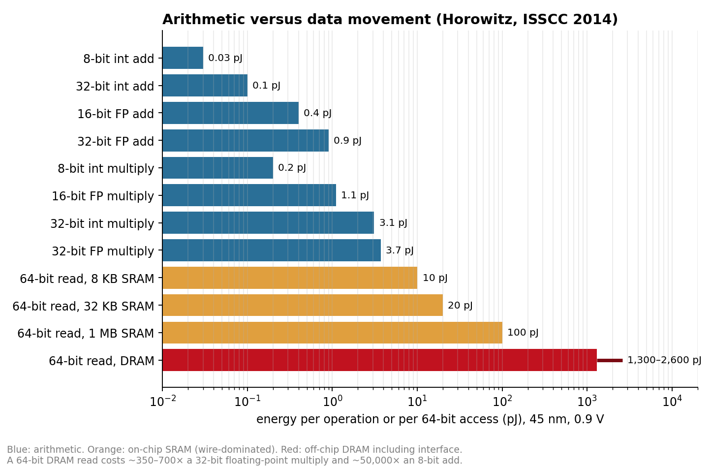
The DRAM access costs 350–700× the floating-point multiply and about 50,000× the 8-bit add. Between 45 nm (2008) and 5 nm-class nodes (2020s), the arithmetic energies fell another ~5–10×; the DRAM energy fell by a comparable factor only where the memory was moved onto the package (HBM). The ratio has not closed.
The time budget looks the same. A 2026 server core executes ~4–6 instructions per cycle at ~0.2 ns per cycle. A DRAM access that misses every cache takes 80–110 ns in a loaded system: 400–500 cycles, or 2,000+ instruction slots. Little's law says that keeping the core busy across such a miss requires ~2,000 instructions in flight; the largest reorder buffers hold 500–700. Out-of-order execution alone cannot bridge the gap; only caches, prefetching and massive multithreading (GPUs) can.
1.5 Checking the standard explanation
The explanation you were given (the "fact-checker" contrasting a 2D-versus-1D intuition pump with interconnect physics) is largely right. Three corrections and two additions:
- The 2D/1D intuition pump is not wrong, just incomplete. It correctly captures that transistor count grows as κ² while the length of the longest wires does not shrink, because die and package sizes did not shrink (die area stayed at the reticle limit of ~800 mm² for high-end parts; a DIMM is still about 13 cm long). The complete statement is: energy = length × (energy per length), and both factors stopped improving — length for geometric reasons, energy per length for the physical reasons the explanation lists.
- "Capacitance per unit length stays flat" is correct, with one lever that also stalled. c can be reduced only by lowering the dielectric constant. The industry went from SiO₂ (k = 3.9, through the 180-nm node) to fluorinated glass (3.6) to carbon-doped oxide (~2.9) to porous ultra-low-k (~2.4–2.6) and, at a few layers, air gaps. Porous dielectrics are mechanically weak and absorb moisture; k has been stuck near 2.5–3.0 since the 32/28-nm nodes (~2011). So even the "flat" c was supposed to fall and did not.
- The V_dd floor is a subthreshold-slope limit, not a thermal-noise limit. A MOSFET's off-current falls by at most one decade per (kT/q)·ln 10 ≈ 60 mV of gate voltage at room temperature, because carriers surmount the channel barrier with a Boltzmann distribution. Getting 10⁴–10⁵ of on/off ratio therefore costs 0.25–0.35 V of threshold, and the transistor needs another ~0.3–0.4 V of overdrive to be fast. That is the origin of the 0.6–0.9 V floor. Thermal noise (kT/C) would allow operation far lower — subthreshold circuits run at 0.2–0.3 V, and the theoretical minimum supply for a CMOS inverter with gain is only ~36 mV at 300 K (Swanson–Meindl) — but they are 10–100× slower. Also, ruthenium is used as a liner and, increasingly, as a barrier-free replacement conductor; tantalum nitride is the barrier that ruthenium replaces.
- Addition: the memory cell itself is a wall. Interconnect physics explains why moving a bit is expensive, but not why DRAM latency stalled at ~30 ns of access and ~48 ns of row cycle. That comes from charge sensing, the retention/leakage constraint on the access transistor, and the unscaled wordline voltage (Section 1.3, Part III).
- Addition: the wall is stacked. On-chip wires (Part IV) are one layer. Package and board signaling (Part V) is another with its own physics (transmission lines, termination, pad capacitance in picofarads). The organization of the memory system (Part VI: row overfetch, refresh, bank parallelism, Rowhammer) is a third. The hierarchy (Part VII) is the response to all of them at once.
Part II — Sixty years, era by era
2.0 Timeline
| Year | Event | Why it matters for the wall |
|---|---|---|
| 1953 | Magnetic-core memory in MIT's Whirlwind (Forrester) | Main memory ~1 µs; the standard for two decades |
| 1962 | Manchester Atlas: virtual memory and paging | The idea of a hierarchy managed automatically |
| 1965 | Moore's "Cramming more components" article; Wilkes's "Slave memories" paper | Density trend named; cache concept invented |
| 1966–68 | Dennard invents the 1T1C DRAM cell (IBM; patent filed 1967, granted 1968) | The cell that would scale for sixty years |
| 1968 | IBM System/360 Model 85: first commercial cache (16–32 KB, 80 ns) against ~1 µs core | The first machine built around a memory wall |
| 1969 | Intel 3101 (64-bit bipolar SRAM) and 1101 (256-bit MOS SRAM) | Semiconductor memory becomes a product |
| 1970 | Intel 1103, 1 Kbit DRAM, 3-transistor cell, ~300 ns access | Kills core by 1972–74 |
| 1973 | Mostek MK4096 (4 Kbit): multiplexed row/column addresses (RAS/CAS) | Halves pin count; locks in the two-step row/column access still used in DDR5 |
| 1974 | Dennard scaling paper | Thirty years of free transistor improvement begin |
| 1976 | Mostek MK4116 (16 Kbit) becomes the industry standard part | Address multiplexing wins |
| 1978–79 | Alpha-particle soft errors discovered (May & Woods, Intel) | Sets the critical-charge floor for cells |
| 1979–81 | 64 Kbit generation; single +5 V supply; Japanese vendors take the lead | DRAM becomes a commodity manufactured by the best fab, not the best designer |
| 1984 | Motorola 68020: first mainstream microprocessor with an on-chip (256-byte) cache | Caches return to the chip |
| 1985–86 | Intel exits DRAM; 1 Mbit generation; trench (TI, IBM) vs. stacked (Hitachi, Fujitsu, NEC) capacitors | Cell capacitor goes 3D because it cannot shrink |
| 1989 | Intel 80486: 8 KB on-chip L1 cache | Every microprocessor now needs a cache |
| 1990 | Hennessy & Patterson, Computer Architecture: A Quantitative Approach | The "processor–memory performance gap" chart |
| 1992–93 | Samsung becomes #1 in DRAM; first synchronous DRAM (Samsung KM48SL2000) | Interfaces become clocked and pipelined |
| 1995 | Wulf & McKee, "Hitting the Memory Wall"; Pentium Pro with in-package L2; Alpha 21164 with on-die L2 | The wall is named; two-level on-package hierarchies |
| 1997 | IBM ships copper interconnect (CMOS 7S); Tera MTA multithreaded supercomputer | Wire resistance relief (one-time); latency tolerance via threads |
| 2000 | DDR SDRAM standard; Rambus RDRAM with Pentium 4 | The Rambus–DDR war: cost and openness beat raw speed |
| 2001 | Ho, Mai & Horowitz, "The Future of Wires" | The definitive interconnect-scaling analysis |
| 2003 | AMD Opteron/Athlon 64: memory controller integrated on the CPU die | Removes one chip crossing (~30–40 ns) from every access |
| 2004 | Patterson, "Latency Lags Bandwidth"; Intel cancels Tejas; Dennard scaling ends | Voltage stops falling → wire energy stops falling |
| 2006 | Berkeley View: "power wall + memory wall + ILP wall = brick wall" | Multicore era begins |
| 2007 | DDR3; Intel 45 nm high-k metal gate; first iPhone (LPDDR) | Mobile memory becomes its own scaling track |
| 2008 | Intel Nehalem: integrated memory controller + shared L3; buried-wordline DRAM (Qimonda) | Three cache levels become standard |
| 2009 | Roofline model (Williams, Waterman, Patterson) | Memory-boundedness gets a picture |
| 2011–13 | Micron HMC (2011); JEDEC HBM standard (Oct. 2013); Samsung 3D V-NAND; Haswell eDRAM L4 | Memory goes vertical (stacking) and L4 appears |
| 2012–13 | Elpida bankruptcy; industry consolidates to Samsung, SK hynix, Micron | Three suppliers for the world |
| 2014 | Horowitz's ISSCC keynote; Rowhammer paper (Kim et al.); DDR4 | Energy numbers and cell-interference failures published |
| 2015 | AMD Fury: first product with HBM; Intel/Micron announce 3D XPoint | Memory on the package; storage-class memory attempted |
| 2017 | Nvidia Volta tensor cores; O'Connor et al. "Fine-Grained DRAM" | Arithmetic gets even cheaper; DRAM overfetch quantified |
| 2019 | CXL 1.0; UPMEM processing-in-memory DIMMs; Optane DIMMs ship | Disaggregation and near-data compute, both as stopgaps |
| 2020 | DDR5 standard; Apple M1 with unified on-package LPDDR | Memory on package goes mainstream |
| 2021 | Samsung HBM-PIM; EUV in DRAM (1α); Cerebras WSE-2 (40 GB on-wafer SRAM) | Compute in memory; memory as the whole chip |
| 2022 | AMD 3D V-Cache (hybrid-bonded SRAM); HBM3 in Nvidia H100; Intel kills Optane; FlashAttention | Cache scaling by stacking; storage-class memory fails; algorithms adapt |
| 2024 | HBM3E; GDDR7; Cerebras WSE-3 (44 GB); Gholami et al. "AI and Memory Wall" | Compute 3×/2yr vs. bandwidth 1.6×/2yr documented |
| 2025 | JEDEC HBM4 spec (April); SK hynix 30-year DRAM roadmap (4F² VG, 3D DRAM); DRAM prices begin surging | The road past 6F² is charted; the economic wall appears |
| 2026 | HBM4 mass production (Samsung Feb., Micron Q1, SK hynix); Nvidia Rubin; TSMC A16 with backside power; DRAM contract prices +90% QoQ in Q1 | Where this report is written |
2.1 Prehistory and the first wall (1950–1968)
Core memory was the first random-access memory that worked at scale. A core plane stored one bit per ferrite ring, read destructively by driving current through it, and cost about $1 per bit in the mid-1950s falling to a cent per bit by 1970. Its cycle time, ~1 µs, was set by the physics of magnetization reversal and the inductance of long drive lines — a wire problem before there were transistors to compare it with.
Processors improved faster. By the mid-1960s, transistorized CPUs had cycle times well under 100 ns while core stayed near 1 µs. Maurice Wilkes's two-page 1965 note "Slave Memories and Dynamic Storage Allocation" proposed a small fast memory that would automatically hold recently used words of the large slow one. IBM built it: the System/360 Model 85 (announced 1968) placed a 16 KB (expandable to 32 KB) "high-speed buffer" between an 80-ns processor and 1.04-µs core. J. S. Liptay's 1968 IBM Systems Journal paper on the Model 85 is where the word "cache" entered the vocabulary. The gap the cache bridged was 13×; the design goal was to make the machine behave as if all of memory ran at buffer speed, and simulations showed hit rates above 95% on real workloads.
The point of recording this is that the memory wall predates the microprocessor. It was there when memory was magnetic and processors were discrete transistors, because it is a property of distance, not of any particular technology.
2.2 The semiconductor memory revolution (1968–1980)
Semiconductor memory did not begin as DRAM. Intel's first products (1969) were static RAMs: the 3101 (64 bits, bipolar) and the 1101 (256 bits, MOS). SRAM was easy to use but consumed six transistors per bit.
Dennard's 1T1C cell — one transistor, one capacitor, invented at IBM in 1966 — was the minimum conceivable. Intel's 1103 (October 1970) used an intermediate three-transistor cell designed by William Regitz at Honeywell and productized by Joel Karp at Intel: 1,024 bits, PMOS, roughly 300 ns access, and notoriously finicky to use (it needed precharge clocks with tight timing, and it needed to be refreshed every two milliseconds). It was also about a cent per bit — the price of core, at a fraction of the space and power. By 1972 the 1103 was the best-selling semiconductor memory in the world and core was finished.
Two decisions made in 1973 still shape every memory access in 2026. Mostek's MK4096 (4 Kbit) was the first DRAM with a true 1T1C cell in volume and the first to multiplex its address pins: the row address is presented first with the Row Address Strobe (RAS), then the column address with the Column Address Strobe (CAS). Robert Proebsting's multiplexing cut the package from 22 to 16 pins and roughly halved the cost of the package and the board, at the cost of forcing a two-step access. Intel and TI initially refused to follow; by the 16 Kbit generation (Mostek's MK4116, 1976) multiplexing had won. The tRCD (RAS-to-CAS delay) that every memory controller still schedules around is Proebsting's 1973 decision, and the row-buffer structure it implies — open a whole row, then pick columns from it — is the reason DRAM access is a page-oriented, overfetching operation to this day.
The 64 Kbit generation (1979–81) brought a single +5 V supply and the arrival of Japanese manufacturers (Fujitsu, Hitachi, NEC, Toshiba, Mitsubishi) with yields and quality the American firms could not match. And in 1978–79 came the first sign that the cell had a physics floor: Intel's Tim May and Murray Woods traced a mysterious rise in soft errors in 16 Kbit parts to alpha particles emitted by trace uranium and thorium in the ceramic package material (the contamination was ultimately traced upstream to a mining region near the ceramic supplier, as the story is usually told). A single alpha particle deposits tens of femtocoulombs along its track in silicon. A cell holding less than a "critical charge" of that order would flip. From then on, DRAM designers had a number they could not scale below.
2.3 The microprocessor era and the gap (1980–1995)
For a few years the wall disappeared. An 8086 at 5 MHz had a 200 ns cycle and took four cycles per bus access; a 150-ns DRAM kept up with one wait state or none. Early PCs had no cache because they needed none. Cycle times fell fast, though: 80286 (1982) at ~100 ns, 80386 (1985) at 62 ns, 80486 (1989) at 40 ns, Pentium (1993) at 15 ns. DRAM access went from ~150 ns to ~70 ns in the same period. In cycles, a miss went from about 1 to about 10.
The caches came back. Motorola's 68020 (1984) carried a 256-byte instruction cache — tiny, but the first on-chip cache in a mainstream microprocessor. Intel's 386 relied on external SRAM caches (the 82385 controller, 1987); the 486 (1989) integrated 8 KB. RISC designs (MIPS R2000, 1986; SPARC) were built around split instruction/data caches from the start, because their whole premise — one instruction per cycle — was impossible without them.
DRAM in the same period moved from 256 Kbit to 16 Mbit, from NMOS to CMOS, and the capacitor went 3D. Two camps formed in the 1 Mbit and 4 Mbit generations: the trench capacitor etched into the substrate (Texas Instruments, IBM, later Toshiba and the Infineon/Qimonda lineage) and the stacked capacitor built above the transistor (proposed by Mitsumasa Koyanagi at Hitachi in 1978; adopted by Hitachi, Fujitsu, NEC, Mitsubishi, and Samsung). Both were responses to the same fact: at a 1-µm feature size a planar capacitor could no longer provide 30 fF. Stacked capacitors won by the 2000s because they scaled better with height. Meanwhile the manufacturing center of gravity moved from the US (Intel exited DRAM in 1985; Micron alone survived) to Japan (over half of world supply by 1986) and then to Korea (Samsung took the #1 position in 1992 and has held it, except briefly in 2025 when SK hynix's HBM business pushed it past Samsung in revenue).
In 1990 Hennessy and Patterson's textbook drew the chart that defined the field's anxiety: processor performance improving 35% per year until 1986 and 55% per year after; DRAM latency improving 7% per year. Two exponentials with different exponents diverge without limit. William Wulf and Sally McKee's four-page note "Hitting the Memory Wall: Implications of the Obvious" (Computer Architecture News, March 1995) did the arithmetic: with those rates, even a cache with a 99% hit rate would see its average access time dominated by misses within about a decade, and no amount of hit-rate improvement could help because the miss cost was growing without bound. They expected the wall to bite around 2005–2010 and asked, rhetorically, whether there was any way around it.
2.4 Naming the wall and building around it (1995–2005)
The industry's answer was: every trick at once.
Latency tolerance in the core. Out-of-order execution (Tomasulo's 1967 algorithm from the IBM 360/91, revived in the PowerPC 604, MIPS R10000 and Pentium Pro in 1995) lets independent instructions proceed while a load waits. Non-blocking caches (Kroft, 1981) allow multiple outstanding misses. Hardware prefetchers guess the next address. Simultaneous multithreading (Tullsen et al., 1995; Intel Hyper-Threading, 2002) lets another thread use the idle issue slots. The most radical answer was Burton Smith's Tera MTA (1997), which had no data cache at all and hid a 150-cycle memory latency by switching among 128 hardware threads every cycle. It was a commercial failure and a conceptual success: it is, in outline, how every GPU works.
More cache, closer. Intel's Pentium Pro (1995) put a 256 KB–1 MB L2 SRAM die in the same package on a private full-speed bus, an expensive dual-cavity ceramic package that Intel abandoned for the Pentium II cartridge (1997) and then re-absorbed onto the die (Celeron 300A, 1998; Pentium III Coppermine, 1999). DEC's Alpha 21164 (1995) had 96 KB of L2 on the die and a third level off it: the first three-level hierarchy in a microprocessor. Itanium 2 (2002) reached 3 MB of on-die L3, later 9 MB.
Faster interfaces, not faster cells. Synchronous DRAM (JEDEC, 1993; PC66/PC100 by 1998) put a clock on the bus and pipelined column accesses. Rambus's RDRAM ran a narrow bus at 400–800 MHz, and Intel bet the Pentium 4 platform on it (1999–2001); the Rambus–DDR war ended with double-data-rate SDRAM (JEDEC, 2000) winning on cost, openness and litigation fatigue. The key fact is that none of these interfaces made the DRAM array faster. Bandwidth per pin rose from ~100 Mb/s (PC100) to 400 Mb/s (DDR-400); tRCD stayed at 15–20 ns.
Copper and low-k. IBM shipped copper interconnect in 1997 (CMOS 7S); everyone followed by 2000. Copper's resistivity (1.7 µΩ·cm) is 40% below aluminum's, and low-k dielectrics started to appear at 130 nm. This was a one-time gift; Part IV explains why it ran out.
Integrating the memory controller. AMD's Opteron (2003) moved the memory controller onto the CPU die, with HyperTransport links between sockets. This removed a full chip crossing (the "northbridge") from every access — the single largest latency improvement of the decade, roughly 30–40 ns — and it is the reason modern latency is 80–100 ns rather than 130–150 ns. Intel followed with Nehalem in 2008.
And then voltage stopped falling. By 2004 Intel's 90-nm Prescott Pentium 4 dissipated over 100 W at 3.8 GHz; its successor Tejas was cancelled. Leakage current, which the subthreshold slope bounds from below, had made further threshold-voltage reduction impossible, and without threshold reduction the supply could not fall without losing speed. Dennard scaling ended. Transistors kept shrinking; their energy stopped falling as κ³ and fell as roughly κ instead. For wires — whose only remaining lever was V² — energy per millimeter stopped falling altogether.
2.5 Multicore and the bandwidth wall (2005–2015)
With frequency capped near 3–4 GHz, performance came from parallelism: dual-core in 2005–06, quad-core by 2007, and manycore GPUs in general-purpose use after CUDA (2007). Parallel cores multiply memory bandwidth demand. Rogers et al. ("Scaling the Bandwidth Wall," ISCA 2009) showed that with pin bandwidth growing far slower than core count, the number of cores that could actually be fed would saturate within a few generations unless caches grew or compression and other tricks were used.
The DRAM interface responded by getting wider and faster on the same array: DDR3 (2007) at 800–1,600 Mb/s per pin; DDR4 (2014) at 1,600–3,200; GDDR5 (2008) at 4–7 Gb/s for GPUs. A DDR3-1600 DIMM delivers 12.8 GB/s; a 2026 DDR5-6400 DIMM delivers 51 GB/s; a 2026 HBM4 stack delivers 2,000–3,300 GB/s. Bandwidth improved ~100× in fifteen years. Row-cycle time did not move.
Three developments in this decade set up everything that followed:
- Memory went vertical. Samsung's 3D V-NAND (2013) turned flash into a stack of 24, then 32, then hundreds of layers. Micron's Hybrid Memory Cube (2011) and JEDEC's High Bandwidth Memory standard (October 2013; first shipped in AMD's Fury GPU in 2015 with SK hynix dies) stacked DRAM dies on through-silicon vias. HBM's 1,024-bit interface at modest per-pin speed, sitting a few millimeters from the processor on a silicon interposer, is the most important memory-system idea since the cache: it attacks length directly. HMC lost (discontinued 2018) because it kept a serial link to the CPU and never became a JEDEC standard.
- eDRAM and L4. IBM's POWER7 (2010) put 32 MB of embedded DRAM L3 on the die; Intel's Haswell (2013) added a 128 MB eDRAM L4 die ("Crystal Well") in the package. Both were early signs that SRAM alone could not keep the hierarchy growing.
- The cell's failure modes multiplied. The RAIDR paper (Liu et al., ISCA 2012) projected that at 64 Gb per chip, refresh alone would consume about half of DRAM throughput and half of its energy if nothing changed. Kim et al. (ISCA 2014) disclosed Rowhammer: repeatedly activating one row flips bits in its neighbors, because at ~20 nm spacing the wordline's electric field disturbs adjacent cells. The activation count needed fell from ~139,000 on 2014 DDR3 parts to as few as ~4,800 on 2020 LPDDR4 parts as cells got closer. Density scaling was now creating reliability problems that cost area, latency and energy to mitigate.
2.6 The AI era: the wall becomes the roofline (2015–2026)
Machine learning changed the shape of demand. A matrix multiply has high arithmetic intensity (many operations per byte fetched) when its operands are large and reused; a transformer decoder generating one token at a time has almost none — each weight is fetched from memory, used once, and discarded. Gholami et al. ("AI and Memory Wall," IEEE Micro, 2024) measured the twenty-year trend: peak server FLOPS up 60,000× (3.0× every two years), DRAM bandwidth up 100× (1.6× every two years), interconnect bandwidth up 30× (1.4× every two years). The ridge point of the roofline — the arithmetic intensity at which a machine becomes compute-bound rather than memory-bound — rose from ~1 FLOP/byte on vector supercomputers to ~300 FLOP/byte for FP16 on an H100 (2022: ~1 PFLOP/s against 3.35 TB/s) and over 1,000 FLOP/byte at FP4 on Blackwell (2024: ~9 PFLOP/s against 8 TB/s).
Every hardware development of the decade is an attempt to move memory closer or make arithmetic cheaper, and the second makes the wall worse:
- Cheaper arithmetic by precision. Tensor cores (Volta, 2017) and each successive generation halved the operand width: FP32 → FP16/BF16 → FP8 (2022) → FP4 (2024). Halving the bits halves the memory traffic and quarters the multiplier energy, so the ratio of fetch cost to compute cost still worsens.
- HBM on every accelerator. HBM2 (2016, ~256 GB/s per stack), HBM2E, HBM3 (2022, ~800 GB/s), HBM3E (2024, ~1.2 TB/s), and HBM4 (2026, 2–3.3 TB/s with a 2,048-bit interface and a logic base die built on a foundry process). Eight stacks on a 2026 GPU package deliver ~20 TB/s. The entire year's HBM4 output was reportedly sold out before it shipped.
- Cache by stacking. AMD's 3D V-Cache (2022) hybrid-bonds a 64 MB SRAM die onto each compute die at ~9-µm pad pitch; a 96-core EPYC "Genoa-X" (2023) carries 1,152 MB of L3. Cerebras's wafer-scale engine (WSE-3, 2024) has 44 GB of SRAM distributed across a 46,000 mm² wafer, with memory bandwidth quoted in petabytes per second, on the theory that the only way to beat the wire is never to leave the die. Groq's LPU (230 MB SRAM, no DRAM) is the same bet at chip scale.
- Memory on the package for everyone. Apple's M1 (2020) put LPDDR on the package; M-series Ultra parts reach ~800 GB/s. Nvidia's Grace-Hopper and Grace-Blackwell put CPU LPDDR5X and GPU HBM behind a coherent link so that HBM acts as a cache for LPDDR.
- Disaggregation. CXL (2019–) attaches DRAM over a PCIe-class serial link at ~200–300 ns, trading latency for capacity and pooling. Intel's Optane (announced 2015 as "1,000× faster than NAND, 10× denser than DRAM"; shipped 2017–2019; cancelled July 2022) tried to fill the gap between DRAM and flash with a new device and could not reach the cost point. The gap is now filled with more DRAM, further away.
- The algorithms adapt. FlashAttention (2022) is the purest example: it recomputes parts of attention rather than storing them, because on an A100 the FLOPs are so cheap that recomputing is faster than a round trip to HBM. Weight quantization to 4 bits, KV-cache compression, speculative decoding, mixture-of-experts sparsity and batching are all ways of spending arithmetic to save bytes.
- The economic wall. HBM uses roughly three times the wafer area per gigabyte of conventional DRAM and commands several times the margin. As the three suppliers shifted wafer starts to HBM in 2025–2026, conventional DRAM contract prices rose about 90–95% quarter-on-quarter in Q1 2026 by TrendForce's estimate, and DDR4 spot prices per gigabit briefly exceeded HBM3E. For the first time in the sixty-year history, the cost per bit of ordinary memory went up substantially for a sustained period. Suppliers have warned that the shortage may last past 2027.
Part III — The cell wall: DRAM in depth
3.1 Density: the curve that worked
| Year | Bits per die | Lead parts / notes | Cell technology |
|---|---|---|---|
| 1970 | 1 K | Intel 1103 (3T cell, PMOS, ~10 µm) | planar, 3 transistors |
| 1973 | 4 K | Mostek MK4096 (1T1C, multiplexed address) | planar 1T1C |
| 1976 | 16 K | Mostek MK4116 (three supplies) | planar |
| 1980 | 64 K | Fujitsu, Hitachi, NEC, TI, Mostek (+5 V only) | planar, ~2–3 µm |
| 1983 | 256 K | NEC, Hitachi, Toshiba | planar, folded bitline |
| 1986 | 1 M | Toshiba, Hitachi, TI (1 µm) | trench / stacked capacitors appear |
| 1989 | 4 M | Japanese leaders; Samsung enters top tier | 3D capacitors universal; CMOS |
| 1992 | 16 M | Samsung #1; first SDRAM | stacked capacitor dominant |
| 1996 | 64 M | Samsung, NEC, Hitachi | hemispherical-grain poly to boost area |
| 1999 | 256 M | Samsung, NEC, Micron (0.18 µm) | Ta₂O₅ / high-k dielectrics begin |
| 2003 | 512 M | DDR/DDR2 era (~90 nm) | recess-channel array transistor (Samsung) |
| 2006 | 1 G | DDR2/DDR3 (~70 nm) | ZAZ (ZrO₂/Al₂O₃/ZrO₂) dielectrics |
| 2009 | 2 G | DDR3 (~50 nm) | buried wordline (Qimonda, then all) |
| 2012 | 4 G | DDR3/DDR4 (~30 nm, "3x nm") | cylinder capacitors, aspect ratio >20 |
| 2015 | 8 G | DDR4 (~20 nm, "2x/1x") | saddle-fin access transistor |
| 2018 | 16 G | DDR4/DDR5 (1y/1z, ~16–17 nm) | quad-patterning; aspect ratio >40 |
| 2021 | 16–24 G | DDR5 (1α, ~14 nm; EUV enters) | 6F² with F ≈ 14 nm |
| 2024 | 32 G | DDR5 (1β/1γ, ~12–13 nm) | supporter lattices for pillars |
| 2026 | 32 G (48–64 G sampling) | DDR5, LPDDR5X/6, HBM4 (1c, ~11–12 nm) | last 6F² generations; 4F² VCT prototypes |
From 1 Kbit to 32 Gbit is a factor of 3.2 × 10⁷. Through the 1990s the industry delivered 4× every three years — Moore's original 1965 observation was, in fact, about memory. After 2010 the cadence slowed to 2× every four to five years, and the "1x/1y/1z/1α/1β/1γ/1c" node names conceal the fact that F has moved only from ~19 nm to ~11 nm in a decade. The remaining planar roadmap is one more node ("1d," ~10 nm, expected 2027–28) before the 6F² cell runs out (SemiAnalysis's VLSI 2025 summary; SK hynix roadmap, VLSI 2025).
3.2 Latency: the curve that did not
Access time is the interval from presenting a row address to receiving data (tRCD + CL in modern terms). Cycle time is the minimum interval between two accesses to the same bank (tRC = tRAS + tRP): the time to open a row, sense it, restore it and precharge the bitlines.
| Year | Generation | Row access (ns) | Column access (ns) | Row cycle (ns) |
|---|---|---|---|---|
| 1980 | 64 Kb | 170–250 | 75 | 250 |
| 1983 | 256 Kb | 150–220 | 50 | 220 |
| 1986 | 1 Mb | 120–190 | 25 | 190 |
| 1989 | 4 Mb | 100–165 | 20 | 165 |
| 1992 | 16 Mb | 80–120 | 15 | 120 |
| 1996 | 64 Mb (EDO) | 70–110 | 12 | 110 |
| 2000 | 256 Mb (PC133) | 65–90 | 7 | 90 |
| 2004 | 1 Gb (DDR/DDR2) | 55–70 | 5 | 70 |
| 2006 | 2 Gb (DDR2) | 50–60 | 2.5 | 60 |
| 2010 | 4 Gb (DDR3-1600) | tRCD ≈ 14; tRCD+CL ≈ 28 | 1 | 48.75 |
| 2018 | 16 Gb (DDR4-3200) | tRCD ≈ 14; tRCD+CL ≈ 28 | 0.6 | 45.75 |
| 2021 | 16 Gb (DDR5-4800) | tRCD ≈ 16; tRCD+CL ≈ 33 | 0.4 | ~48 |
| 2026 | 32 Gb (DDR5-6400 / HBM4) | tRCD ≈ 14–16; tRCD+CL ≈ 30 | 0.3 | 45–50 |
(1980–2006 rows adapted from the survey table in Hennessy & Patterson, Computer Architecture: A Quantitative Approach; 2010–2026 rows from JEDEC timing bins for the named speed grades. "Column access" here is the per-word transfer interval, which improved enormously through pipelining and burst transfer; the row numbers are the latency.)
Row access improved 6–8× in 46 years (Figure 1b). Row cycle improved 5×, all of it before 2010. Since then the DRAM array has been flat: every generation of DDR and HBM has raised the clock and widened the bus while the array underneath runs at the same speed, and CAS latency in nanoseconds has actually crept upward with DDR5.
3.3 Why the array is slow: a walk through one activation
- Precharge. Bitlines are equalized to V_core/2 (~0.5–0.55 V). The bitline is a wire hundreds of cells long with ~20–40 fF of capacitance.
- Wordline activation. The row decoder drives the wordline to V_PP (2.5–3 V). The wordline is a polysilicon/tungsten line with thousands of transistor gates hanging off it; modern designs use hierarchical (main/sub) wordlines and buried wordlines to cut its RC, but its RC delay is still several nanoseconds.
- Charge sharing. Each cell's ~10–20 fF dumps its charge onto its bitline. The bitline moves by ΔV = (V_core/2)·C_S/(C_S+C_BL) ≈ 100–200 mV. This is a passive RC process governed by the access transistor's on-resistance and the bitline capacitance.
- Sensing. A cross-coupled latch amplifies the differential to full rail. Sense-amplifier offset (tens of millivolts, from threshold-voltage mismatch) sets the minimum ΔV and hence the minimum C_S.
- Column access. The requested columns are gated from the sense amplifiers onto local I/O lines, then global I/O lines running across the die, then through the output drivers.
- Restore. The sense amplifiers write the full-rail value back into every cell in the row (the read was destructive). tRAS, ~30–35 ns, is dominated by this restore because the capacitor must be charged through the access transistor's resistance.
- Precharge again. tRP ≈ 13–15 ns.
Steps 2, 3, 4, and 6 are analog RC processes on long lines; step 5 is a global wire. Nothing in the list is a logic gate whose delay Dennard scaling would have reduced. This is why shrinking F from 1 µm to 11 nm — a factor of 90 — cut tRC by only 5×, and why DRAM vendors never marketed speed: the customer paid for bits.
3.4 The capacitor: forced into the third dimension
The stored charge must satisfy three constraints:
- Sensing: C_S/(C_S + C_BL) large enough for ΔV ≥ ~100 mV.
- Retention: leakage × 64 ms < ~⅓ of the charge.
- Radiation: charge greater than the critical charge Q_crit an ionizing particle can deposit (tens of fC for alphas; neutron-induced events later became the dominant concern as alpha sources were cleaned up).
With V_core/2 ≈ 0.55 V, a 15 fF cell holds ~8 fC ≈ 50,000 electrons. The capacitance target fell from ~30 fF (1990s) to ~10–15 fF (2020s) only because shorter bitlines cut C_BL and better sense amplifiers cut the required ΔV.
Meanwhile the cell footprint went from ~1,500 µm² (1103) to ~0.001 µm² (6F² at F ≈ 12 nm): six orders of magnitude. Holding 15 fF in a footprint of ~(2F)² ≈ 600 nm² requires, with a k ≈ 35 dielectric ~6 nm thick, a plate area of about 0.3 µm² — 500× the footprint. Hence the cylinder: a pillar ~30 nm across and 1–1.5 µm tall, with both inner and outer surfaces used, held upright by lattice-like supporters so that it does not topple during processing, and lined with a ZrO₂/Al₂O₃/ZrO₂ dielectric and TiN electrodes. Aspect ratios approach 50:1. This is the physics that ends 6F²: the pillars cannot get taller and thinner indefinitely, the dielectric cannot get thinner without tunneling leakage, and higher-k materials tend to have smaller bandgaps and hence more leakage. The exits are 4F² vertical-channel-transistor cells (one more ~30% density step) and then 3D DRAM, in which cells are laid horizontally and stacked like 3D NAND — trading the aspect-ratio problem for a layer-count problem.
3.5 The access transistor and the wordline that would not scale
The transistor must deliver ~50 fA of off-current and enough on-current to restore the cell within tRAS. The industry solved short-channel leakage at 90 nm with the recess-channel array transistor (Samsung, 2003), then buried wordlines (Qimonda, 2008), then saddle-fin structures, which lengthen the channel below the surface so that a 20-nm-pitch device can behave like a 100-nm-channel device. The price is a wordline that must swing to V_PP ≈ 2.5–3 V (generated by on-die charge pumps at ~30–50% efficiency) and to a negative off-level (~–0.2 V) to suppress leakage. A logic wire swings 0.75 V; energy scales as V², so the wordline's per-unit-capacitance energy is ~16× that of a logic wire — before counting the pump's inefficiency.
3.6 Refresh: a tax that grows with density
JEDEC requires every row to be refreshed within 64 ms (32 ms above 85 °C, because leakage roughly doubles per 10 °C). A DDR4 chip issues an all-bank refresh every 7.8 µs; each takes tRFC ≈ 350 ns at 8 Gb and 550 ns at 16 Gb, during which the chip cannot serve requests — 4.5% to 7% of all time, and rising with capacity. Liu et al. (2012) showed that at 64 Gb per chip, unmodified refresh would consume roughly half of throughput and half of energy. DDR5 answers with per-bank and same-bank refresh, more banks (32 per chip), and on-die ECC to tolerate the weakest cells; HBM adds per-pseudo-channel scheduling. Each is an organizational patch over the same physics: charge leaks, and there are more cells every generation to top up.
3.7 Rowhammer and interference: density creates new failure modes
When rows sit ~20 nm apart, the field from an activated wordline and the charge injected by its transistors disturb neighboring cells; repeated activation drains them before their refresh. Kim et al. (2014) needed ~139,000 activations in 64 ms to flip a bit in DDR3; by 2020 (Kim et al., "Revisiting RowHammer," ISCA 2020) LPDDR4 parts flipped at ~4,800. Mitigations (target-row refresh, refresh-management commands in DDR5, per-row activation counters, and in 2024–26 in-DRAM trackers) all cost area, bandwidth or latency. The same story — variable retention time, sense-amp mismatch at small sizes, and the need for on-die ECC in DDR5 — shows density scaling actively degrading the parameters that determine speed and energy.
Part IV — The on-chip wire wall
4.1 Reverse scaling in numbers
Take the 2001 "Future of Wires" analysis forward to 2026. A minimum-pitch wire at the 180-nm node (1999) was about 250 nm wide and 500 nm tall; at a 3-nm-class node (2023) the tightest metal pitch is ~20–24 nm, so the wire is ~10–12 nm wide. The cross-section fell by ~500×, so resistance per length rose ~500× for the same metal. Capacitance per length stayed at 0.15–0.25 fF/µm. A 1-mm wire that had ~1 ns of unrepeated RC delay in 1999 would have ~500 ns today; in practice it is broken into segments a few tens of micrometers long with a repeater at each break, and its effective delay is set by the repeaters (a few tens of picoseconds per segment). A 2004 study (Saxena et al., IEEE TCAD) projected that repeaters alone could occupy tens of percent of a chip's cells by the 32-nm node; the estimate proved roughly right for high-frequency designs.
4.2 Copper runs out
Copper's advantage over aluminum was 40% in bulk resistivity (1.7 vs 2.7 µΩ·cm). At small dimensions two size effects erase it. The electron mean free path in copper is ~39 nm at room temperature; when a wire's dimensions approach that, electrons scatter off the surfaces (Fuchs–Sondheimer) and at grain boundaries, which become more frequent as grains are forced smaller (Mayadas–Shatzkes). At 10–15 nm linewidths, effective resistivity is 4–6× bulk. On top of that, copper needs a diffusion barrier (TaN) and a liner (Ta, Co, Ru) totalling 3–5 nm, which do not scale and consume half the cross-section of a 12-nm line. Net: a leading-edge M0/M1 line has ~8–10× the resistivity of the bulk copper the industry adopted in 1997.
The responses have been incremental: cobalt at the lowest layers (Intel, 2018); ruthenium as a liner and, at the tightest pitches, as a barrier-free replacement conductor (its bulk resistivity is 7 µΩ·cm, worse than copper's, but its mean free path is ~7 nm so it stops degrading where copper has already lost); molybdenum for similar reasons; subtractive etching instead of damascene fill; and air gaps at selected layers. Backside power delivery (Intel's PowerVia in 18A, shipping in 2026 products; TSMC's Super Power Rail in A16, entering production in 2026) moves the power grid to the back of the wafer, which relieves routing congestion and IR drop but does nothing for signal-wire RC — Intel's ISSCC 2025 paper noted that putting backside power inside an SRAM cell would actually enlarge it.
4.3 Low-k stalls
The capacitance term has only one knob, k. The industry moved from SiO₂ (3.9) to FSG (3.6, ~2001) to SiCOH (2.9–3.0, ~2004) to porous SiCOH (2.4–2.6, ~2009). Below about 2.4, porous films crack during chemical-mechanical polishing, delaminate in packaging, and absorb moisture that raises k back up. Progress stopped near 2.5. Air gaps (k ≈ 1) are used at a few layers where geometry permits. Effective k in a 2026 stack is about the same as in 2011.
4.4 Voltage stalls — the master lever
Everything above concerns delay and the c term. The energy of a wire is ½cLV², and after 2005 V froze. Supply voltage fell from 5 V (1980s) to 3.3 V (1993), 2.5 V (1997), 1.5 V (2000), 1.2 V (2005), 1.0 V (2010), and then ~0.75–0.85 V (2015–2026). From 1980 to 2005 V fell 4× (energy 16×); from 2005 to 2026 it fell ~1.4× (energy 2×). Had Dennard scaling continued, V in 2026 would be ~0.15 V and wire energy per millimeter ~30× lower than it is. The floor is the subthreshold slope (Section 1.5). Gate-all-around nanosheets (2022–2026) and stacked CFETs (2030s) improve electrostatics and may permit ~0.5–0.6 V; negative-capacitance and tunnel FETs that would break the 60 mV/decade limit remain laboratory devices after two decades of effort.
4.5 The consequence in one number
Energy per bit per millimeter on chip, from about 2005 to 2026: ~0.05–0.1 pJ, flat. Energy per 8-bit multiply-accumulate over the same period: from ~0.5 pJ to ~0.03 pJ, down ~15×. Crossing a 20-mm die (1–2 pJ/bit) is now 30–60× an 8-bit MAC per bit moved; a 64-bit word crossing the die costs the same as several thousand 8-bit MACs. This is why every 2026 accelerator is a grid of small tiles with local SRAM, and why "data movement" — not arithmetic — is the line item designers optimize.
Part V — The off-chip wall
5.1 Leaving the die changes the physics
On-chip, a signal charges femtofarads through resistive wires. Off-chip, it must drive a bond pad (hundreds of femtofarads), a package trace and ball (a picofarad-scale load and a transmission line), a board trace of centimeters, and a receiver with its own pad — and, at gigabit rates, the line must be terminated to a characteristic impedance (~40–50 Ω) to absorb reflections, which dissipates static current regardless of activity. A DDR4 I/O at 1.2 V burns roughly 10–20 pJ per bit at the interface alone; add the DRAM core (activation, sensing, on-die routing) and system-level figures of 20–40 pJ/bit for DDR4 and 40–70 pJ/bit for DDR3 were typical (O'Connor et al., 2017, and vendor power calculators).
Propagation delay, incidentally, is not the problem. A signal travels ~15–18 cm/ns in board dielectric; a DIMM 8 cm from the socket costs ~0.5 ns each way, a few CPU cycles out of ~450. The off-chip wall is charging capacitance and RC/protocol serialization, not the speed of light.
5.2 Pins do not scale
A chip's transistor count grows as κ² per node; its perimeter and package area do not. Rent's rule says required I/O grows as a power (~0.5–0.7) of gate count, so a chip is always short of pins. Intel's Socket 7 (1995) had 321 pins; LGA775 (2004) 775; LGA2011 (2011) 2,011; LGA4677 (2023) 4,677; LGA7529 (2024) 7,529. About 25× in thirty years, against 10⁴× more transistors. Each DDR channel consumes ~150 signal pins for 64 (72 with ECC) data bits; a server CPU with 12 channels devotes roughly a third of its package to memory. This is the "pin wall."
5.3 Every interface since 2013 shortens the wire
| Interface | Year | Where the DRAM sits | Distance | Bits wide | Per-pin rate | Approx. system energy/bit |
|---|---|---|---|---|---|---|
| DDR3 | 2007 | DIMM on board | 5–10 cm | 64/channel | 0.8–1.6 Gb/s | 40–70 pJ |
| DDR4 | 2014 | DIMM on board | 5–10 cm | 64/channel | 1.6–3.2 Gb/s | 20–40 pJ |
| GDDR5/6 | 2008/2018 | soldered next to GPU | 2–4 cm | 32/device | 7–16 Gb/s | 8–20 pJ |
| LPDDR4/5X | 2014/2021 | soldered or on package | 0.5–3 cm | 16–32/channel | 4–8.5 Gb/s | 5–15 pJ |
| DDR5 (incl. MRDIMM) | 2020 | DIMM on board | 5–10 cm | 2×32/channel | 4.8–8.8 Gb/s | 10–25 pJ |
| HBM2/2E | 2016/2019 | on interposer beside die | 2–8 mm | 1,024/stack | 2–3.6 Gb/s | ~4 pJ |
| HBM3/3E | 2022/2024 | on interposer beside die | 2–8 mm | 1,024/stack | 6.4–9.6 Gb/s | 2.5–3.5 pJ |
| HBM4 | 2026 | on interposer, logic base die | 2–8 mm | 2,048/stack | 8–13 Gb/s | vendors claim ~20–40% below HBM3E (~2 pJ) |
| Hybrid-bonded SRAM (V-Cache) | 2022 | stacked on the die | <100 µm vertical | thousands of TSVs | on-chip rates | ~0.1–0.3 pJ (est.) |
| On-chip, 1 mm | — | same die | 1 mm | — | — | 0.05–0.1 pJ |
(Energy figures are approximate system-level values — DRAM core plus interface — from O'Connor et al. 2017, vendor materials, and published estimates; they vary with access pattern and configuration. The "wide and slow" strategy of HBM is precisely a wire-length strategy: HBM4's 2,048 bits at ~8–13 Gb/s deliver 2–3.3 TB/s per stack across a few millimeters of silicon interposer, at per-pin speeds a DDR5 DIMM would find unremarkable.)
The row is monotonic: the closer the memory, the cheaper the bit. The improvement from DDR3 to HBM3E — roughly 15–20× — came almost entirely from geometry (distance from centimeters to millimeters) and modest voltage reduction, not from transistor scaling. The next factor of ten requires the next step in geometry: DRAM hybrid-bonded directly on top of logic, where the vertical distance is tens of micrometers.
5.4 Thermal coupling: the power wall meets the memory wall
Putting memory next to a 1,000-W GPU has a cost the tables above do not show. DRAM retention halves roughly every 10 °C above the JEDEC 85 °C threshold, doubling refresh. HBM stacks are limited in height (12-high in 2026, 16-high being qualified) partly by thermal resistance through the stack. Energy per bit inside the stack becomes heat that raises refresh and lowers margin, a feedback loop that caps how much bandwidth can be packed into a package.
Part VI — The organization wall
6.1 Overfetch: the 8-kilobit row
Because of the 1973 row/column design, a DRAM activation opens an entire row — 8 kilobits (1 KB) per ×8 chip, 8 KB across an 8-chip rank — into the sense amplifiers. A processor that wanted one 64-byte cache line with no row-buffer locality moved 8 KB of charge to get 64 B: an overfetch of 128×. Activation and precharge energy is on the order of a nanojoule per device per row. O'Connor et al. (MICRO 2017) measured that in an HBM2 device most access energy is spent in activation/precharge and on-die data movement rather than in the actual interface, and proposed "fine-grained DRAM" with narrower rows. Wider rows were originally chosen to amortize the wordline decoder and sense-amplifier area; they are an organizational choice that made density cheaper and random access more expensive.
6.2 Bank parallelism: buying latency tolerance with area
Since the array cannot get faster, the only way to raise throughput per chip is to have more independent arrays. DDR (2000) had 4 banks; DDR3 8; DDR4 16 in bank groups; DDR5 32; HBM3 up to 64 per stack across 16 pseudo-channels; HBM4 32 channels. Each bank carries its own sense amplifiers (which are large — sense amplifiers and decoders are a substantial fraction of a DRAM die) and its own timing constraints (tRRD, tFAW) to limit peak current. Memory controllers reorder hundreds of requests to exploit bank parallelism and row-buffer hits; the controller's queueing is itself a source of tens of nanoseconds of latency in loaded systems.
6.3 Where the 90 nanoseconds go
A 2026 server load miss, from core to DRAM and back, roughly:
| Stage | Approx. time |
|---|---|
| L1 miss, L2 lookup | 3–4 ns |
| L3 lookup across the die-spanning mesh/ring, coherence check | 20–35 ns |
| Memory controller queue and scheduling | 5–20 ns (load dependent) |
| Off-chip transfer, PHY, DIMM | 5–10 ns |
| DRAM tRCD + CL (row already closed) | 28–33 ns |
| Return path | 5–10 ns |
| Total | ~80–110 ns |
Only about a third is the DRAM array. Another third is on-chip wire and coherence machinery; the rest is queueing and interface. Every stage is wire or protocol; none is arithmetic.
6.4 The GPU's answer: don't wait
A datacenter GPU sees ~500–700 ns to HBM (measured by microbenchmarks; the long path includes address translation, crossbar and the HBM PHY). It does not try to hide this with reordering; it keeps ~100,000–250,000 threads resident and switches among them, exactly as the Tera MTA did in 1997. The cost is that the machine only works when there is that much parallel work — which is why batch size, not clock speed, is the first knob an inference engineer turns.
Part VII — The hierarchy: from no caches to caches everywhere
7.1 Sixty years of caches
| Year | Machine | Hierarchy (sizes) | Largest-cache latency | Main memory latency |
|---|---|---|---|---|
| 1965 | Typical mainframe/mini | registers → core | — | ~1 µs |
| 1968 | IBM S/360 Model 85 | 16–32 KB buffer (first cache) | 80 ns | 1.04 µs |
| 1978 | DEC VAX-11/780 | 8 KB cache | 200 ns | ~1.2 µs (effective) |
| 1980 | IBM PC / 8086-class | none | — | ~200–300 ns |
| 1984 | Motorola 68020 | 256 B on-chip I-cache | 1 cycle | ~150 ns |
| 1987 | Intel 386 + 82385 | 32–64 KB external | ~2 cycles | ~150 ns |
| 1989 | Intel 486 | 8 KB on-chip L1 | 1 cycle | ~100 ns |
| 1993 | Intel Pentium | 8+8 KB L1; 256 KB board L2 | ~3–5 cycles | ~100 ns |
| 1995 | Pentium Pro / Alpha 21164 | 8+8 KB L1; 256 KB–1 MB L2 in package / 96 KB L2 on die + up to 64 MB L3 | ~7 cycles | ~130 ns |
| 1999 | Pentium III (Coppermine) | 16+16 KB; 256 KB L2 on die | ~7 cycles | ~130 ns |
| 2002 | Itanium 2 | 16+16 KB; 256 KB; 3 MB L3 on die | ~12 cycles | ~150 ns |
| 2006 | Core 2 Duo | 32+32 KB; 4 MB shared L2 | ~14 cycles | ~100 ns |
| 2008 | Intel Nehalem | 32+32 KB; 256 KB; 8 MB shared L3 + IMC | ~40 cycles | ~65–80 ns |
| 2010 | IBM POWER7 | + 32 MB eDRAM L3 | ~25 ns | ~100 ns |
| 2013 | Intel Haswell (Crystal Well) | + 128 MB eDRAM L4 | ~40 ns | ~80 ns |
| 2015 | IBM z13 | 960 MB eDRAM L4 per node | ~100+ ns | ~200 ns |
| 2020 | Apple M1 | 192+128 KB L1; 12 MB L2; 16 MB SLC; LPDDR on package | ~40 ns | ~100 ns |
| 2022 | AMD EPYC Milan-X | 32+32 KB; 512 KB; 768 MB L3 (3D V-Cache) | ~14–15 ns | ~100 ns |
| 2023 | AMD EPYC Genoa-X | 1,152 MB L3 per socket | ~14–15 ns | ~100 ns |
| 2024 | Cerebras WSE-3 | 44 GB on-wafer SRAM, no DRAM | ~1 cycle (local) | — |
| 2026 | Typical server | µop cache; 48–64 KB L1; 1–2 MB L2; 32–1,152 MB L3; optional HBM/LPDDR "L4"; DDR5; CXL; NVMe | 10–40 ns (L3) | 80–110 ns (DDR5), 200–300 ns (CXL) |
The largest cache per socket grew from 16 KB to 1,152 MB — 72,000× — while its latency improved from 80 ns to ~15 ns, about 5×. The same law that governs DRAM governs SRAM: capacity scales, wires do not.
7.2 SRAM stopped scaling too
| Node (year) | High-density 6T bitcell (µm²) | Scaling vs. prior |
|---|---|---|
| 180 nm (1999) | ~5.6 | — |
| 130 nm (2001) | ~2.45 | 0.44× |
| 90 nm (2004) | ~1.0 | 0.41× |
| 65 nm (2006) | ~0.57 | 0.57× |
| 45 nm (2008) | 0.346 | 0.61× |
| 32 nm (2010) | 0.171 | 0.49× |
| 22 nm (2012) | 0.092 | 0.54× |
| 14 nm (2014) | 0.050 | 0.54× |
| 10 nm / N7 (2017–18) | 0.031 / 0.027 | ~0.6× |
| N5 (2020) | 0.021 | 0.78× |
| N3E (2023) | 0.021 | 1.0× — no shrink |
| N2 (2025) | 0.0175 | 0.83× |
| Intel 18A (2025–26) | 0.021 (HD), 0.023 (HP) | 0.88× vs Intel 3 |
(Sources: Intel and TSMC IEDM/ISSCC disclosures as reported; TSMC N2 and Intel 18A both quote ~38 Mb/mm² macro density at ISSCC 2025.)
A 6T cell is six minimum-size transistors that must read without flipping and write without failing across billions of copies. Its stability depends on the matching of threshold voltages, and mismatch grows as 1/√(W·L) as devices shrink (Pelgrom's law): random dopant fluctuation and line-edge roughness make small transistors unpredictable. The cell therefore cannot use the smallest transistors the process offers, cannot lower its supply voltage (V_min for SRAM is typically higher than for logic), and cannot shrink its contacts and wires below the pitch limits that also bound logic. From 2020 onward the bitcell has been shrinking by ~10–20% per node instead of the historical 50%, which is why:
- AMD builds its V-Cache dies on an older, cheaper node (N7/N6 class) and stacks them on the compute die: SRAM that stopped scaling laterally now scales vertically.
- Intel and AMD move L3 onto separate "base" or "cache" chiplets.
- Accelerators are designed as tiles with SRAM sized by the area they can afford rather than the capacity they need.
7.3 Why the number of levels grows
A hierarchy level is worthwhile if it is several times faster than the level below and large enough to catch most misses from the level above. With a typical ratio of 4–6× per level and a total gap G between register and main memory, the number of levels is about log(G)/log(5). In 1980 (G ≈ 1–2) that is zero levels; in 1995 (G ≈ 20) it is two; in 2008 (G ≈ 200) three; in 2026 (G ≈ 500 to DDR5, ~1,500 to CXL, ~500,000 to NVMe) four to five cache levels plus memory and storage tiers. Every widening of the gap adds roughly one tier per factor of five. The tiers are not a design fashion; they are the shape of the gap.
7.4 The machinery of tolerance
Alongside the caches, the mechanisms that hide latency have grown to grotesque proportions:
- Reorder buffers: 40 entries (Pentium Pro, 1995) → 224 (Skylake, 2015) → 448–576 (Zen 5, Lion Cove, 2024) → 600+ (Apple's cores). Little's law says a 5-wide core at 450 cycles of miss latency would need ~2,000 to cover one miss; the ROB has never caught up and never will.
- Outstanding misses: L1 miss-status holding registers went from 4–8 to 16–48; L2/L3 queues to hundreds. Memory-level parallelism, not single-miss latency, determines throughput.
- Prefetchers: stream, stride, spatial, temporal and in 2026 learned prefetchers consume a measurable share of core area and memory bandwidth.
- Threads: two per core on CPUs (SMT); tens of thousands per die on GPUs.
- Software: loop tiling/blocking (Lam, Rothberg & Wolf, 1991), cache-oblivious algorithms (Frigo et al., 1999), the GotoBLAS approach to dense linear algebra, the roofline model as the standard mental picture, and IO-aware kernels like FlashAttention that count HBM bytes, not FLOPs.
Part VIII — The compute side: why arithmetic became almost free
For completeness, the other half of the divergence, in three phases:
- Dennard (1975–2005). Energy per gate switch fell as κ³, ~10⁴× over the period; clock frequency rose ~1,000× (from ~1 MHz to ~3 GHz); instruction-level parallelism added another ~4×.
- Post-Dennard scaling (2005–2016). Voltage froze; energy per gate fell roughly with capacitance (~κ per node); frequency froze; performance came from multiplying cores.
- Specialization and precision (2016–2026). Tensor cores, systolic arrays and reduced precision. An 8-bit integer multiply-accumulate costs ~0.2–0.25 pJ at 45 nm (Horowitz) and ~0.02–0.05 pJ at 5-nm-class nodes; a 4-bit operation less still. The most efficient 2026 accelerators execute on the order of 10¹⁵ low-precision operations per second per kilowatt.
Rough estimates of the ratio, for a 64-bit main-memory read versus a 32-bit multiply, over the decades:
| Era | 64-bit DRAM read (system level) | 32-bit multiply (circuit level) | Ratio |
|---|---|---|---|
| mid-1980s (5 V, ×1 DRAMs on a board) | ~0.1–1 µJ | ~2–5 nJ | ~100× |
| 2014 (Horowitz, 45 nm, DDR3) | 1.3–2.6 nJ | 3.7 pJ | ~500× |
| 2026, DDR5 | ~1 nJ | ~0.3 pJ | ~3,000× |
| 2026, HBM3E/HBM4 | ~0.15–0.2 nJ | ~0.3 pJ | ~500–700× |
| 2026, per 8-bit weight vs. 8-bit MAC | ~16–24 pJ (HBM) | ~0.03 pJ | ~500–800× |
The last row is the number that governs large-language-model inference: each weight fetched from HBM must be reused across ~500–1,000 multiply-accumulates (i.e., tokens in a batch) before the machine is compute-bound. Below that, the accelerator's arithmetic units are idle and the workload is "memory-bound" — which is the memory wall, restated for 2026.
Part IX — Projections, 2026–2040
9.1 What is already committed (2026–2029)
These are on published roadmaps with silicon in qualification or production:
- DRAM: the 1c node (~11–12 nm) is in volume in 2026; 1d (~10 nm) follows in 2027–28 and is expected to be the last 6F² generation. Samsung and SK hynix are prototyping 4F² vertical-channel/vertical-gate cells with the periphery wafer-bonded under the array, which yields ~30% more bits per area at the same F; Micron is reported to be skipping 4F² for direct 3D DRAM. Per-die capacity: 32 Gb mainstream, 48–64 Gb arriving.
- HBM: HBM4 (2,048-bit, 8–13 Gb/s per pin, 2–3.3 TB/s per stack, 12-high with 16-high in qualification, 36–64 GB per stack, foundry-built logic base dies) is in production at all three vendors as of mid-2026; HBM4E with larger capacity and custom base-die logic is planned for 2027. Hybrid bonding replaces microbumps in the stack around 2027–2029, cutting stack height and thermal resistance. Nvidia's Rubin (2026) and its successors, and the hyperscaler ASICs, will each carry 8–16 stacks.
- DDR/LPDDR: DDR5 to 8,800 MT/s with multiplexed-rank DIMMs; LPDDR6; DDR6 in JEDEC definition for late-decade introduction.
- Interconnect: ruthenium/molybdenum at the lowest metal levels and backside power delivery (Intel 18A, TSMC A16) in 2026–27; TSMC A14 in 2028; Intel 14A risk production in 2028. None of this lowers c or V; expect on-chip wire energy to remain ~0.05–0.1 pJ/bit/mm.
- SRAM: ~10–15% bitcell shrink per node; stacked cache dies become common in CPUs and GPUs.
- Disaggregation: CXL 3.x memory pooling in hyperscale deployment; CXL memory as a "far" tier at 200–300 ns.
- Photonics: co-packaged optics in network switches (2025–26) and, by 2027–28, for GPU-to-GPU scale-up fabrics. Energy ~1–3 pJ/bit today, distance-independent.
9.2 Likely (2029–2035)
- 3D DRAM in production, first at 16–32 layers, using horizontally oriented 1T1C cells or capacitor-less gain cells (2T0C) with oxide-semiconductor (IGZO) channels whose leakage is low enough to relax refresh by 10–100×. Per-die capacity moves to 128–256 Gb and the cost-per-bit curve resumes a gentler decline. Latency does not improve; the long vertical/horizontal lines and layer-select decoding may add a few nanoseconds.
- Memory-on-logic. HBM base dies with real compute (reduction, gather/scatter, decompression, KV-cache management) on foundry nodes; DRAM stacked directly on the accelerator die with hybrid bonding at 1–3 µm pitch, giving millions of vertical connections and energy per bit in the 0.1–0.5 pJ range — the first order-of-magnitude improvement in main-memory access energy since the move from DIMM to interposer.
- Optical I/O to memory. Optical links from accelerators to remote HBM/DRAM pools, making capacity a rack-level rather than package-level resource. Bandwidth-per-watt improves; latency does not (photonic links add serialization and conversion, typically ≥100 ns end to end).
- SRAM by stacking only. Lateral bitcell scaling nearly stops (CFET may give one more ~20–30% step in the early 2030s); cache capacity grows through more stacked layers on older nodes.
- Voltage to ~0.5–0.6 V with CFETs and better electrostatics, giving one last ~2× on wire energy.
9.3 Speculative (2035–2040)
- Cryogenic operation. At 77 K the subthreshold slope falls to ~15–20 mV/decade and copper's resistivity drops several-fold; both attack the wire wall directly. Cooling overhead and packaging make it a datacenter-scale question, not a chip-scale one.
- Steep-slope devices (tunnel FETs, negative-capacitance FETs) breaking the 60 mV/decade barrier at usable currents — attempted since the mid-2000s, still unproven in production.
- Non-charge memories in the hierarchy. Embedded MRAM is in production as a flash replacement; spin-orbit-torque MRAM as a last-level cache remains plausible but has not displaced SRAM. Ferroelectric memories (FeRAM, FeFET) are candidates for low-refresh dense embedded memory.
- Analog and in-memory compute for low-precision inference (multiplication by physics inside the array), which sidesteps the wall for the specific operations it can express.
- Monolithic 3D: logic and memory tiers fabricated sequentially on one wafer with nanometer-scale vias, the theoretical end state in which the "wire to memory" is as short as a wire to the next gate.
9.4 A quantitative projection
| Metric | 2026 | 2030 (projected) | 2035 (projected) | Basis |
|---|---|---|---|---|
| DRAM cell / node | 6F², F ≈ 11–12 nm | 4F² VCT, F ≈ 9–10 nm; first 3D DRAM | 3D DRAM, 32–128 layers | vendor roadmaps |
| Max bits per die | 32 Gb (48–64 sampling) | 64–96 Gb | 128–512 Gb | |
| DRAM row cycle (tRC) | 45–50 ns | 45–50 ns | 45–55 ns | cell physics unchanged |
| Loaded latency, core → DDR | 80–110 ns | 80–110 ns | 70–110 ns | wires and protocol |
| HBM bandwidth per stack | 2–3.3 TB/s | 4–6 TB/s | 8–16 TB/s | ~2× per ~3 years |
| HBM energy per bit | ~2 pJ | 1–1.5 pJ | 0.3–0.8 pJ | hybrid bonding, direct stacking |
| DDR channel bandwidth | 51–70 GB/s | 100–140 GB/s (DDR6) | 200+ GB/s | interface cadence |
| On-chip wire, pJ/bit/mm | 0.05–0.1 | 0.05–0.1 | 0.03–0.08 | c flat; V floor ~0.5 V |
| SRAM HD bitcell | 0.0175–0.021 µm² | ~0.015 µm² | ~0.010 µm² | 10–15%/node; CFET |
| 8-bit MAC energy | ~0.03 pJ | ~0.015 pJ | ~0.008 pJ | process + design |
| Accelerator ridge point (low precision) | ~1,000 FLOP/byte | 1,500–2,500 | 3,000+ | 3.0×/2 yr vs 1.6×/2 yr |
| Hierarchy tiers (server) | 8–10 | 9–11 | 9–12 | log of the gap |
| DRAM cost per bit | ~2× the 2024 low | volatile; 3D DRAM resets the curve | slow decline | supply/demand + 3D |
9.5 What will not change
- The DRAM row cycle. Charge sharing and restore through a leakage-limited transistor are physics, not engineering. Expect 45–50 ns for as long as DRAM is a capacitor.
- Energy per millimeter of wire at fixed voltage. The only escapes are shorter wires (3D) and no wires (photons).
- The ratio's direction. Arithmetic will keep getting cheaper through specialization and precision reduction faster than any memory improvement. The memory wall is not a problem awaiting a solution; it is the permanent design constraint of computing, and the design discipline that grew up around it — locality, hierarchy, reuse, recomputation — is now the core of the field.
9.6 Scenarios
- Baseline (most likely). Bandwidth scales ~2× per generation by widening and stacking; latency flat; energy per bit improves ~2× per 4–5 years through packaging; costs rise. Algorithms carry the load: the FLOP-per-byte of deployed workloads rises to match the hardware, through quantization, sparsity, batching and recomputation.
- Upside: 3D integration lands early. DRAM-on-logic hybrid bonding in volume by ~2031 gives a step change in energy per bit (≥5×) and bandwidth (≥5×) for accelerators, turning main memory into something that behaves like a very large L3. Latency still flat.
- Downside: economics and heat bind first. HBM continues to absorb wafer capacity; DRAM cost per bit stops falling for most of the decade; thermal limits cap stack heights; systems ration memory as they once rationed compute. The "memory wall" becomes primarily a supply problem.
Appendix A — Derivations and reference physics
A.1 Dennard scaling. Scale L, W, t_ox, V by 1/κ and doping by κ. Saturation current I ∝ (W/L)·C_ox·(V−V_t)² ∝ 1·κ·κ⁻² = κ⁻¹. Gate capacitance C ∝ WL/t_ox ∝ κ⁻¹. Delay ∝ CV/I ∝ κ⁻¹·κ⁻¹/κ⁻¹ = κ⁻¹. Power ∝ IV ∝ κ⁻². Density ∝ κ², so power density is constant. Energy per switch ∝ CV² ∝ κ⁻³.
A.2 Wire RC. r = ρ/(WH) per unit length; c ≈ ε·f(W/S, H/S) per unit length, invariant under uniform shrink; parallel-plate estimate for a wire between neighbors and ground gives c ≈ 0.15–0.25 fF/µm for k = 3–4 at aspect ratios near 2. Distributed RC delay of an unrepeated line: t ≈ 0.38·r·c·L². With optimal repeaters (segment length ∝ √(R_dC_d/(rc))), delay becomes linear in L at ~ 2L·√(0.38·rc·R_dC_d) plus repeater delays.
A.3 Wire energy. E = ½·c·L·V² per transition (full swing). With c = 0.2 pF/mm and V = 0.8 V: 64 fJ/mm. Realized values 0.05–0.1 pJ/bit/mm including repeaters; ~1–2 pJ across a 20-mm die.
A.4 Copper size effects. Fuchs–Sondheimer surface scattering and Mayadas–Shatzkes grain-boundary scattering: ρ_eff/ρ₀ ≈ 1 + (3/8)(1−p)(λ/d) + grain term, with λ ≈ 39 nm for Cu at 300 K, d the wire dimension, p the specularity. At d ≈ 10–12 nm, ρ_eff ≈ 4–6ρ₀, and the barrier/liner (3–5 nm total) halves the conductive cross-section. Ru (ρ₀ ≈ 7 µΩ·cm, λ ≈ 7 nm) and Mo (ρ₀ ≈ 5 µΩ·cm, λ ≈ 11 nm) cross over below ~12–17 nm.
A.5 Subthreshold slope. I_off ∝ exp(q(V_gs−V_t)/(n·kT)); SS = n·(kT/q)·ln 10 ≥ 59.6 mV/decade at 300 K, with n = 1 + C_dep/C_ox ≥ 1 (practical 63–75 mV/decade). Five decades of on/off → V_t ≥ 0.3 V; adding ~0.3–0.4 V of overdrive for speed → V_dd ≈ 0.6–0.75 V. Minimum V_dd for a static CMOS gate with gain > 1: ~2(kT/q)·ln 2 ≈ 36 mV (Swanson–Meindl), usable only at very low speed.
A.6 DRAM sensing. ΔV_BL = (V_core/2)·C_S/(C_S+C_BL). C_S = 15 fF, C_BL = 30 fF, V_core = 1.1 V → ΔV ≈ 180 mV. Stored charge Q = C_S·V_core/2 ≈ 8 fC ≈ 5×10⁴ electrons. Retention: allowable leakage ≈ (Q/3)/64 ms ≈ 40 fA. Critical charge for soft errors: tens of fC (alpha) — the reason Q could not scale.
A.7 Capacitor geometry. C = ε₀·k·A/t. For 15 fF with k = 35, t = 6 nm: A ≈ 0.29 µm². A cylinder of diameter 30 nm and height h using both surfaces has A ≈ 2π(30 nm)h → h ≈ 1.5 µm; aspect ratio ≈ 50.
A.8 Refresh overhead. Fraction of time busy = tRFC/tREFI = 350 ns/7.8 µs ≈ 4.5% (8 Gb DDR4), 550/7,800 ≈ 7% (16 Gb); doubles above 85 °C.
A.9 Little's law for latency tolerance. In-flight instructions needed = issue width × miss latency (cycles) = 5 × 450 ≈ 2,250, versus reorder buffers of 450–650. GPUs substitute threads: ~10⁵ resident threads × (a few outstanding loads each) ≫ latency × bandwidth.
A.10 Tier count. Levels ≈ log(G)/log(ratio per level); G = 500, ratio = 5 → 3.9 levels of cache between register and DRAM.
A.11 Roofline ridge point. Ridge = peak FLOP/s ÷ peak bytes/s. H100: ~989 TFLOP/s FP16 dense ÷ 3.35 TB/s ≈ 295 FLOP/byte. B200: ~9 PFLOP/s FP4 dense ÷ 8 TB/s ≈ 1,100 FLOP/byte. Cray-1 (1976): 160 MFLOP/s ÷ 640 MB/s ≈ 0.25 FLOP/byte.
Appendix B — Glossary of the timing parameters that did not scale
- tRCD (RAS-to-CAS delay): time from activating a row to being able to read a column from it. ~14–16 ns since 2005.
- CL (CAS latency): time from the column command to first data. ~13–17 ns since 2005.
- tRAS: minimum time a row must stay open (restore). ~32–35 ns.
- tRP: precharge time. ~13–15 ns.
- tRC = tRAS + tRP: row cycle. ~45–50 ns.
- tRFC: refresh cycle time; grows with density (350 → 550 ns from 8 to 16 Gb).
- tREFI: refresh interval; 7.8 µs (3.9 µs above 85 °C).
- tFAW / tRRD: limits on activation rate, set by peak-current (charge-pump) constraints.
References and further reading
Primary sources for the historical and physical claims above, in roughly chronological order:
- M. V. Wilkes, "Slave Memories and Dynamic Storage Allocation," IEEE Trans. Electronic Computers, EC-14(2), 1965.
- J. S. Liptay, "Structural aspects of the System/360 Model 85, II: The cache," IBM Systems Journal, 7(1), 1968.
- R. H. Dennard, "Field-effect transistor memory," U.S. Patent 3,387,286 (filed 1967, granted 1968).
- R. H. Dennard et al., "Design of Ion-Implanted MOSFETs with Very Small Physical Dimensions," IEEE J. Solid-State Circuits, SC-9(5), 1974.
- T. C. May and M. H. Woods, "Alpha-Particle-Induced Soft Errors in Dynamic Memories," IEEE Trans. Electron Devices, ED-26(1), 1979.
- D. Kroft, "Lockup-Free Instruction Fetch/Prefetch Cache Organization," ISCA, 1981.
- J. L. Hennessy and D. A. Patterson, Computer Architecture: A Quantitative Approach, 1st ed. 1990; 6th ed. 2017 (DRAM timing survey table, Ch. 2).
- M. S. Lam, E. E. Rothberg, M. E. Wolf, "The Cache Performance and Optimizations of Blocked Algorithms," ASPLOS, 1991.
- W. A. Wulf and S. A. McKee, "Hitting the Memory Wall: Implications of the Obvious," ACM SIGARCH Computer Architecture News, 23(1), 1995.
- M. T. Bohr, "Interconnect Scaling — The Real Limiter to High Performance ULSI," IEDM, 1995.
- D. M. Tullsen, S. J. Eggers, H. M. Levy, "Simultaneous Multithreading: Maximizing On-Chip Parallelism," ISCA, 1995.
- R. Ho, K. W. Mai, M. A. Horowitz, "The Future of Wires," Proc. IEEE, 89(4), 2001.
- V. Agarwal, M. S. Hrishikesh, S. W. Keckler, D. Burger, "Clock Rate versus IPC: The End of the Road for Conventional Microarchitectures," ISCA, 2000.
- P. Saxena et al., "Repeater Scaling and Its Impact on CAD," IEEE Trans. CAD, 23(4), 2004.
- D. A. Patterson, "Latency Lags Bandwidth," Communications of the ACM, 47(10), 2004.
- K. Asanović et al., "The Landscape of Parallel Computing Research: A View from Berkeley," UC Berkeley Tech. Rep. UCB/EECS-2006-183, 2006.
- B. Jacob, S. Ng, D. Wang, Memory Systems: Cache, DRAM, Disk, Morgan Kaufmann, 2008.
- S. Williams, A. Waterman, D. Patterson, "Roofline: An Insightful Visual Performance Model for Multicore Architectures," CACM, 52(4), 2009.
- B. M. Rogers et al., "Scaling the Bandwidth Wall: Challenges in and Avenues for CMP Scaling," ISCA, 2009.
- W. J. Dally, "Power, Programmability, and Granularity: The Challenges of ExaScale Computing," keynote, IPDPS, 2011 (energy-per-operation and per-wire figures).
- J. Liu, B. Jaiyen, R. Veras, O. Mutlu, "RAIDR: Retention-Aware Intelligent DRAM Refresh," ISCA, 2012.
- Y. Kim et al., "Flipping Bits in Memory Without Accessing Them: An Experimental Study of DRAM Disturbance Errors," ISCA, 2014.
- M. Horowitz, "Computing's Energy Problem (and What We Can Do About It)," ISSCC, 2014.
- M. O'Connor et al., "Fine-Grained DRAM: Energy-Efficient DRAM for Extreme Bandwidth Systems," MICRO, 2017.
- J. S. Kim et al., "Revisiting RowHammer: An Experimental Analysis of Modern DRAM Devices and Mitigation Techniques," ISCA, 2020.
- T. Dao et al., "FlashAttention: Fast and Memory-Efficient Exact Attention with IO-Awareness," NeurIPS, 2022.
- A. Gholami, Z. Yao, S. Kim, C. Hooper, M. W. Mahoney, K. Keutzer, "AI and Memory Wall," IEEE Micro, 2024 (arXiv:2403.14123).
- JEDEC, JESD79-4/-5 (DDR4/DDR5), JESD235/238 (HBM/HBM3), JESD270-4 (HBM4, April 2025).
Contemporary sources consulted for the 2025–2026 state of the industry:
- SK hynix, "SK hynix Presents Future DRAM Technology Roadmap at IEEE VLSI 2025" (press release, June 2025) — 4F² vertical-gate platform and 3D DRAM as the two pillars beyond 10 nm.
- SemiAnalysis, "Intel 18A Details & Cost, Future of DRAM 4F2 vs 3D, Backside Power Adoption…" (VLSI 2025 coverage) — 6F² scaling ends at 1d; storage-node-contact margin as the limiting factor.
- IEEE Spectrum, "Intel and TSMC Detail SRAM at ISSCC 2025" — 38 Mb/mm² on both 18A and N2; backside power does not shrink the bitcell.
- Micron, "HBM4" product page (2026) — 2,048-bit interface, >11 Gb/s per pin, >2.8 TB/s per stack, pJ/bit improvement versus HBM3E 12-high.
- Siemens EDA blog, "HBM3E and HBM4: IC design guide" (April 2026) — HBM4 architecture, 2.0–3.3 TB/s per stack, 16-high/64 GB stacks.
- Utmel, "HBM4 and the Shift to Customized AI Memory" (June–Aug. 2026) — JEDEC baseline 8 Gb/s and ~2 TB/s; Samsung 3.3 TB/s and Micron 2.8 TB/s products; all three vendors in production by August 2026.
- TrendForce press releases (Oct. 2025, June 2026) — conventional DRAM contract price increases; HBM wafer share of DRAM output (~18%/22%/30% for 2025/26/27); crowding-out dynamics.
- Findchips / Supplyframe Commodity IQ (June 2026) and Counterpoint/Gartner as reported — DDR5 contract price increases of ~50–57% QoQ in 1H 2026; DDR4 spot per-Gb prices exceeding HBM3E; Gartner's ~130% 2026 DRAM price-rise projection.
- IEEE Spectrum, "Interconnects Are in Need of a Major Overhaul" (IEDM 2022 coverage) — ruthenium, top-via, air-gap and backside-power directions.
- The Register, "TSMC says first 1.6nm chips coming in 2026" (April 2024) — A16 with Super Power Rail backside power.
Numbers not attributed to a specific source are the author's engineering estimates from the physics in Appendix A and public datasheets; they should be read as order-of-magnitude values.