Charge, capacitance, repeaters, and the square-root rules: a first-principles reconstruction of the numbers in "On the Model of Computation" (CACM, September 2022)
Technical note. September 2026. The companion figure is embedded in Section 8; tap it to open full size.
Reading guide. Section 0 lists every number Bill Dally gives in "On the Model of Computation: Point" (CACM 65(9), Sept. 2022) next to the value reconstructed here. Sections 1–7 build the physics up from charge to repeated wires and arrive at his two transport constants, 30 fJ per bit-millimeter and 2.5 mm/ns. Sections 8–12 apply them to his memory, sub-array, off-chip and arithmetic figures, including the two square-root rules. Section 13 is a recipe, with code, for regenerating the numbers for any process. Section 14 lists the caveats. The hardware is inferred, not stated by Dally: everything below is consistent with a 5-nm-class CMOS process at about 0.75 V, circa 2021–22.
0. The numbers to be justified
Dally's article makes a single argument: arithmetic has become almost free while communication has not, so a model of computation without a notion of location mis-prices everything by orders of magnitude. He supports it with roughly a dozen figures. Each is reconstructed in this report from a handful of physical constants.
| Dally's figure (as stated) | Reconstructed here | Section |
|---|---|---|
| Energy to move data on chip (implied): 57.4 pJ for 64 bits over 30 mm | 30 fJ per bit-mm = ½·c·V² × activity, with c ≈ 0.2 fF/µm, V ≈ 0.75 V | 2, 3, 7 |
| Speed of on-chip communication (implied): 30 mm in 12 ns | 2.5 mm/ns ≈ c/120 = 1 / (2.5·√(R₀C₀·r·c)), the optimally repeated wire | 5, 6 |
| 8 KB (64 Kb) sub-array: 64-bit access = 0.64 pJ, 300 ps | ≈10 fJ/bit and ≈300 ps from wordline, bitline, sense-amp and decoder budgets | 9 |
| 256 MB memory ≈ 100 mm² | 20 Mb/mm² from a 0.021 µm² 6T cell and ~2.3× array overhead | 10 |
| 256 MB access = 58 pJ, 12.3 ns (57.4 pJ, 12 ns communication; 15 mm each way) | 0.64 pJ + 64 b × 30 mm × 30 fJ = 58.2 pJ; 0.3 ns + 30 mm / 2.5 mm/ns = 12.3 ns | 8, 10 |
| Core at center of a 2 MB array: local 64-bit access = 1 mm round trip, 1.9 pJ, 400 ps | mean center-to-point distance L/2 = 0.5 mm; 64 b × 1 mm × 30 fJ = 1.92 pJ; 1 mm / 2.5 = 0.4 ns | 8 |
| Random on-chip access on a 16 mm die = 21.3 mm | mean round-trip Manhattan distance between random points = 4L/3 = 21.33 mm | 8 |
| Off-chip access = 640 pJ per 64 bits | 10 pJ/bit board-level link (termination + SerDes + both ends) | 11 |
| Average random access ≈ 680 pJ; random / local = 354× | 640 + 21.3 mm × 64 b × 30 fJ = 681 pJ; 681 / 1.92 = 354 | 8, 11 |
| "Add" vs. global memory access = 64,000× | ~10 fJ for an integer add at 5 nm vs 640 pJ | 12 |
| Store vs. recompute: 640 pJ per 16-bit activation; recompute wins below n ≈ 4,000 | 16-bit MAC ≈ 0.16 pJ at 5 nm; 640 / 0.16 = 4,000 | 12 |
| Local vs. random summation = 230× (energy) | (681 + 0.64 + ~0.4) / (1.92 + 0.64 + ~0.4) ≈ 230 with a ~0.4 pJ 64-bit add | 12 |
The whole table follows from six constants: wire capacitance per unit length c, wire resistance per unit length r, supply voltage V, an inverter time constant R₀C₀, SRAM density D, and an off-chip link energy e_io. The rest is geometry.
1. The hardware Dally had in mind
Dally does not name a process. The numbers pin it down well enough:
| Parameter | Value consistent with the article | Evidence |
|---|---|---|
| Process | 5-nm-class FinFET (TSMC N5 generation), 2020–22 | 10 fJ integer add; 20 Mb/mm² SRAM; Dally's NVIDIA research chips of 2021–22 used N5 |
| Supply voltage V | ≈ 0.75 V (0.7–0.8) | 30 fJ/bit-mm with c = 0.2 fF/µm requires V² ≈ 0.55 V² at 50% activity |
| SRAM bit cell | 6T high-density ≈ 0.021 µm² | 256 MB in 100 mm² is 20.5 Mb/mm² ≈ 47 Mb/mm² raw × ~45% array efficiency |
| Sub-array | 64 Kb = 8 KB, 256 × 256 (or 128 × 512) | stated; ≈ 50 µm × 60 µm at the cell size above |
| Die | 16 mm × 16 mm = 256 mm²; 256 cores; 2 MB SRAM per core (1 mm² per core) | stated |
| System | 4 × 4 array of dies with board-level chip-to-chip links | stated; 640 pJ per 64-bit off-chip access |
| Wire capacitance c | ≈ 0.2 fF/µm (0.15–0.25) | geometry (Section 3); the figure has held since the 0.5-µm generation |
| Wire resistance r | ≈ 5–20 kΩ/mm on intermediate metal; 1–3 kΩ/mm on global metal | geometry plus copper size effects (Section 4) |
| Inverter time constant R₀C₀ | ≈ 4–6 ps | FO4 delay ≈ 10–14 ps at 5 nm |
| Transport energy | 30 fJ per bit per mm | derived (Section 7) |
| Transport velocity | 2.5 mm/ns (0.4 ns/mm) | derived (Section 6) |
| Off-chip link energy e_io | 10 pJ/bit | typical board-level SerDes/parallel-link budgets |
2. Charge, capacitance, and what a bit costs
Charge. Electric charge is the conserved quantity carried by electrons (−1.6 × 10⁻¹⁹ C each). A digital "1" on a wire is a surplus of charge that holds the wire at the supply voltage; a "0" is the wire discharged to ground. Sending a bit is therefore not an abstraction: it is physically moving a definite number of electrons onto or off a conductor.
Capacitance. Any conductor separated from other conductors by an insulator can hold charge, and the amount it must hold to sit at voltage V is proportional to V:
Q = C · V
The proportionality constant C is the capacitance, measured in farads (coulombs per volt). It depends only on geometry and on the insulator's permittivity ε: bigger conductors closer together have more capacitance. A wire on a chip, surrounded by other wires and oxide, is a capacitor whether or not anyone wanted it to be; so is a transistor's gate; so is a DRAM cell, deliberately.
How many electrons. A transistor gate at 5 nm has C ≈ 0.05–0.1 fF; at 0.75 V it holds ≈ 300–500 electrons. A 1-mm wire at 0.2 fF/µm has C = 200 fF and holds ≈ 940,000 electrons. Moving one bit across one millimeter requires the driver to supply about two thousand times the charge that switching a transistor does. That ratio — not anything about transistor speed — is the origin of Dally's "communication dominates."
Energy. Charging a capacitor from 0 to V through any resistance draws Q·V = C·V² from the supply, of which ½CV² ends up stored on the capacitor and ½CV² is dissipated as heat in the resistance on the way in. Discharging it dissipates the stored ½CV² as heat too. Per 0→1→0 cycle the supply pays C·V²; per transition, ½CV². Two facts matter for everything that follows:
- The dissipated energy does not depend on the resistance. Lowering R makes the charging faster, not cheaper. This is why copper (1997) and the coming ruthenium and molybdenum lines help delay but do nothing for energy; only C and V do.
- Energy is paid per transition, not per bit sent. Random data toggles a wire on about half the bits, so the average energy per bit is ½ × ½CV² = ¼CV². This "activity factor" α ≈ 0.5 is the single most important reason Dally's constant is 30 fJ and not 60.
So the cost of a bit on a wire is
E_bit = α · ½ · C · V² = α · ½ · (c · L) · V²,
proportional to length through c·L, and to V². Dennard scaling once lowered V every generation; since ~2005 it has fallen only from ~1.1 V to ~0.75 V, and c (next section) does not scale at all. That is why the transport constant is nearly the same in a 2022 article as in Dally's 2010 talks, once the voltage and activity conventions are matched.
3. Wire capacitance per unit length: why it is 0.2 fF/µm in every process
Model a wire of width W and thickness H, at spacing S from its neighbors on the same layer and distance T from the metal layers above and below (which, in a dense chip, are effectively ground planes on average). Treating each face as a parallel-plate capacitor:
c ≈ ε · [ 2·(H/S) + 2·(W/T) ] + fringing
Every term is a ratio of lengths. Shrink W, H, S and T together by any factor and c is unchanged. Capacitance scales with linear size, so capacitance per unit length is a pure shape factor times ε.
Put in the numbers for a typical dense-routing layer: H = 2W (aspect ratio 2), S = W, T = H, and a carbon-doped oxide with k ≈ 3.0 (ε = 3.0 × 8.85 × 10⁻¹² F/m = 2.66 × 10⁻¹¹ F/m):
- lateral (to the two neighbors): 2 × ε × (H/S) = 2 × 2.66 × 10⁻¹¹ × 2 = 1.06 × 10⁻¹⁰ F/m = 0.106 fF/µm
- vertical (to the layers above and below): 2 × ε × (W/T) = 2 × 2.66 × 10⁻¹¹ × 0.5 = 0.027 fF/µm
- fringing fields add roughly 30–50%
Total ≈ 0.13 × 1.4 ≈ 0.18–0.20 fF/µm. The same computation with SiO₂ (k = 3.9) gives ~0.25 fF/µm, which is why the number has been "about 0.2 fF/µm" from the 1990s (SiO₂, wider wires, aspect ratio ~1) to the 2020s (low-k, narrower wires, aspect ratio ~2): the two trends cancelled. The only lever is k, and k stalled near 2.5–3.0 around 2010 because more porous dielectrics could not survive polishing and packaging.
The lateral term dominates. Two-thirds of a dense wire's capacitance is to its neighbors on the same layer, which is also why crosstalk, not ground capacitance, sets the worst-case switching energy (a wire switching opposite to both neighbors sees roughly twice its nominal c).
4. Wire resistance per unit length: the term that does scale, the wrong way
r = ρ / (W · H)
Both dimensions in the denominator shrink with the process, so r grows as the square of the shrink factor. On top of that, copper's resistivity is not the bulk 1.7 µΩ·cm once wires are narrower than the electron mean free path (~39 nm): surface and grain-boundary scattering raise it, and the barrier/liner (3–5 nm total) that copper needs takes a fixed bite out of the cross-section.
Two wire classes matter for Dally's numbers:
| Wire class | W × H | ρ_eff | r | Used for |
|---|---|---|---|---|
| Intermediate (M4–M6 class, ~70 nm pitch) | 35 nm × 70 nm | ≈ 4.5 µΩ·cm | 4.5e-8 / 2.45e-15 = 1.8 × 10⁷ Ω/m ≈ 18 kΩ/mm | wide buses across a memory or core array |
| Global (upper layers, ~0.3 µm pitch) | 150 nm × 300 nm | ≈ 2.5 µΩ·cm | 2.5e-8 / 4.5e-14 = 5.6 × 10⁵ Ω/m ≈ 0.6 kΩ/mm | a few long clocks, power, and signals |
A 64-bit bus crossing a 10-mm array cannot all be on the thick global layers (there are only a few of them and they are mostly power and clock), so the realistic transport resistance is in the intermediate range: 5–20 kΩ/mm. With c = 0.2 pF/mm, the product rc is 1–4 ns/mm², the figure that drives everything in the next two sections.
5. The distributed RC line: why unrepeated wires fail as L²
A long wire is not a lumped capacitor charged through one resistor; it is a chain of many small resistors and capacitors. Charge injected at one end must flow through the resistance of the first segment to charge the second segment's capacitance, then through both to reach the third, and so on. The Elmore (first-moment) estimate of the 50% delay is
t_wire ≈ 0.38 · r · c · L² (≈ 0.4·RC for a distributed line vs 0.69·RC for a lumped one)
The delay grows with the square of the length, because both the total resistance and the total capacitance are proportional to L.
Numbers for the intermediate wire of Section 4, rc = 18 kΩ/mm × 0.2 pF/mm = 3.6 ns/mm²:
| Length | Unrepeated delay |
|---|---|
| 100 µm | 0.38 × 3.6 × 0.01 = 14 ps |
| 1 mm | 1.4 ns |
| 10 mm | 137 ns |
| 15 mm | 308 ns |
An unrepeated 15-mm wire in a 5-nm process would take a third of a microsecond — a thousand clock cycles. Even on the thick global wire (rc ≈ 0.12 ns/mm²) 15 mm is 10 ns unrepeated. This is the "reverse scaling" of interconnect: rc per unit length has grown with every node, so any wire of fixed length has been getting slower for twenty-five years. The way out is to break the L² law.
6. Repeaters and the first square-root rule
What a repeater is. An ordinary CMOS inverter (or a pair, to preserve polarity) inserted along the wire. It does no logic; it just receives the degraded, slowly rising signal from the previous segment and re-drives the next segment from the supply rail. It converts one long RC diffusion into a chain of short ones plus gate delays.
Why it works. Split a wire of length L into k segments. Each segment's RC delay is 0.38·r·c·(L/k)², so all k segments together take 0.38·r·c·L²/k — the wire delay falls as 1/k. But each repeater adds its own delay, roughly a gate delay τ_g ≈ 0.7·R₀C₀ (R₀ and C₀ being the on-resistance and capacitance of a reference inverter; τ_g is a few picoseconds at 5 nm). Total:
T(k) ≈ 0.38·r·c·L²/k + k·(0.7·R₀C₀ + loading terms)
Minimizing over k (Bakoglu, 1990) gives the classic results:
- optimal number of repeaters: k_opt = L · √(0.4·r·c / (0.7·R₀C₀))
- optimal segment length: L_seg = √(0.7·R₀C₀ / (0.4·r·c))
- minimum delay: T_min ≈ 2.5 · √(R₀C₀ · r·c) · L
That is the first square-root rule. The delay of an optimally repeated wire is linear in its length, and the constant of proportionality is the geometric mean of the gate time constant and the wire time constant per unit length. A wire behaves like a signal traveling at a definite velocity:
v = 1 / (2.5 · √(R₀C₀ · r·c))
The numbers (Figure 1a). Take R₀C₀ ≈ 5 ps (FO4 ≈ 12 ps at 5 nm) and rc = 3.6 ns/mm²:
- √(5 × 10⁻¹² s × 3.6 × 10⁻⁹ s/mm²) = √(1.8 × 10⁻²⁰ s²/mm²) = 1.34 × 10⁻¹⁰ s/mm
- T_min/L = 2.5 × 0.134 ns/mm = 0.34 ns/mm → v ≈ 3.0 mm/ns ≈ c/100
- L_seg = √(0.7 × 5 ps / (0.4 × 3.6 ns/mm²)) = √(2.4 × 10⁻³ mm²) ≈ 50 µm between repeaters
With slightly denser wire (rc = 5 ns/mm²) or a slower gate (R₀C₀ = 6 ps): 0.43 ns/mm → 2.3 mm/ns ≈ c/130. On the thick global wire the same formula gives ~0.06 ns/mm (16 mm/ns), but there is not enough of it to carry buses. Real interconnects also pipeline every few millimeters (a flip-flop costs a clock-cycle boundary) and arbitrate at routers, so the effective velocity of a 64-bit transaction is 0.35–0.5 ns/mm. Dally's 30 mm in 12 ns is 0.40 ns/mm, 2.5 mm/ns, c/120: exactly the middle of this range. Your c/160 (0.53 ns/mm) is the same physics with the pipelining overhead counted a little more generously.
Why this velocity does not improve with scaling. In the product R₀C₀ · r·c, each node makes R₀C₀ smaller (faster transistors) and r·c larger (thinner wires), by roughly the same factor. The geometric mean barely moves. Repeated-wire delay per millimeter has sat within a factor of two of 0.3 ns/mm since the 130-nm node (2001), which is why a 2022 article, a 2010 talk, and a 2026 grid model can all use a velocity near c/120 and none of them is out of date. Meanwhile gate delay fell ~10× over the same period: the ratio of communication time to computation time is what keeps growing.
Why it is not the speed of light. Electromagnetic waves in the on-chip dielectric travel at c/√k ≈ c/1.7 ≈ 175 mm/ns. Dally's signals are ~70× slower because on-chip wires are RC lines, not transmission lines: their resistance per unit length is so high that the inductive/wave regime never applies at these lengths. Off-chip traces on a board are transmission lines and do propagate near c/2, which is why the off-chip cost (Section 11) is energy, not delay per millimeter.
What repeaters cost. Each repeater's input and output capacitance is charged along with the wire. For optimally sized repeaters the extra capacitance is typically 20–40% of the segment's wire capacitance, so the energy per bit-mm rises by that fraction; the repeaters also occupy silicon (in aggressive designs, a noticeable percentage of all cells). They buy linear delay at the price of extra energy — there is no free lunch in the energy term because, as Section 2 showed, energy depends only on total C and V.
7. The transport constant: 30 fJ per bit-millimeter
Assemble Sections 2, 3 and 6:
e_w = α · ½ · (c_wire + c_rep) · V²
| Case | c_wire | repeater overhead | V | α | e_w |
|---|---|---|---|---|---|
| Bare wire, full activity | 0.20 fF/µm | 0 | 0.75 V | 1.0 | 56 fJ/bit-mm |
| Bare wire, random data | 0.20 | 0 | 0.75 | 0.5 | 28 |
| With repeaters, random data | 0.20 | +30% | 0.75 | 0.5 | 37 |
| With repeaters, random data, low V | 0.20 | +30% | 0.65 | 0.5 | 27 |
| Dally (implied) | — | — | — | — | 30 (57.4 pJ ÷ 64 b ÷ 30 mm = 29.9 fJ) |
| Older rule of thumb (28–45 nm, ~0.9–1.0 V, α ≈ 1) | 0.20 | +30% | 1.0 | 1.0 | ~130 → "0.1 pJ/bit-mm" |
| Your grid: 1 fJ/byte/µm | (c_eff ≈ 0.39 fF/µm at α = 1) | 0.8 | 1.0 | 125 |
Dally's 30 fJ is "0.2 fF/µm, three-quarters of a volt, random data, modest repeater overhead." The familiar 0.1 pJ/bit-mm from the 2010s is the same wire at a higher voltage with every bit charged to full swing. Any model that quotes an energy per bit-mm should therefore state its (V, α, repeater) convention; the physics supports anything from ~25 to ~130 fJ depending on those three choices, and the difference is exactly the 3–4× that separates your model from Dally's.
Two useful corollaries of the constant:
- Distance equivalents. 30 fJ/bit-mm means a 64-bit word costs 1.92 pJ per millimeter. Every other cost can be quoted in millimeters: a sub-array read (0.64 pJ) is 0.33 mm; an off-chip access (640 pJ) is 333 mm — the length of twenty dies; an integer add (10 fJ) is 5 µm, the width of a few standard cells.
- Electrons per bit-mm. At 0.75 V, 30 fJ is 40 fC of charge moved per bit per millimeter on average: a quarter of a million electrons.
8. Memory is a two-dimensional object: the second square-root rule
A memory of N bits at density D bits/mm² occupies area A = N/D, a square of side L = √(N/D). Any access must travel from the requester to the bit and back. Whatever the layout, the distance is some fixed fraction κ of L that depends only on where the requester sits and what statistic you charge:
| Requester → target (Manhattan metric, uniform targets in an L × L square) | Mean one-way distance | Round trip |
|---|---|---|
| Random point → random point | 2L/3 | 4L/3 |
| Center → random point | L/2 | L |
| Midpoint of an edge → random point | 3L/4 | 3L/2 |
| Corner → random point | L | 2L |
| Corner → far corner (worst case) | 2L | 4L |
(For a uniform variable on [0, L], E|x − y| = L/3 and E|x − L/2| = L/4; Manhattan distance adds the two axes.)
Combining with the transport constants gives the general heuristic for a b-bit access:
E(N) ≈ E₀ + b · e_w · 2κ · √(N/D) and t(N) ≈ t₀ + 2κ · √(N/D) / v
with E₀ ≈ 0.64 pJ and t₀ ≈ 0.3 ns for the terminal sub-array (Section 9). Energy and latency grow as the square root of capacity (Figure 1b): every 4× in memory size costs 2× in access energy and 2× in access time. This is the rule Dally has used in talks for fifteen years and it is why cache hierarchies are geometric: a level four times larger is twice as slow and twice as costly to reach, so each level should be sized where the reuse it captures pays for that factor of two.
Now check Dally's three distances:
- 2 MB tile with the core at its center (1 mm × 1 mm): κ = ½, one way 0.5 mm, round trip 1 mm — his stated figure. Energy 64 b × 1 mm × 30 fJ = 1.92 pJ; time 1 mm / 2.5 mm/ns = 0.40 ns. Both match exactly (he charges pure transport here, no E₀/t₀).
- Random access on a 16-mm die: κ = 2/3 each way, round trip 4L/3 = 4 × 16/3 = 21.33 mm — his stated 21.3 mm to three digits. Energy 64 × 21.33 × 0.03 = 41 pJ; time 8.5 ns.
- 256 MB block (10 mm × 10 mm), 15 mm each way: 15 mm = 1.5 L does not come from any mean in the table. It is the 87.5th percentile of the corner-to-random distance (P(x + y ≤ d) = 1 − (2L − d)²/2L² = 0.875 at d = 15), or equivalently a requester sitting ~5 mm outside the block on a larger die and reading a random location. Read it as a deliberately conservative, near-worst-case figure. With it, energy = 0.64 + 64 × 30 × 0.03 = 58.2 pJ and time = 0.3 + 30/2.5 = 12.3 ns, his numbers. With the other conventions, the same memory gives:
| One-way distance | Convention | Energy | Latency |
|---|---|---|---|
| 6.7 mm | random ↔ random | 26 pJ | 5.6 ns |
| 10 mm | corner → random (mean) | 39 pJ | 8.3 ns |
| 15 mm | Dally (≈ 88th percentile from a corner) | 58 pJ | 12.3 ns |
| 20 mm | corner → far corner (worst) | 77 pJ | 16.3 ns |
This is the source of the "coincidence" in your grid model: charging the mean over a half-diamond (2R/3 with R = 16.4 mm gives 10.9 mm each way) is a different statistic from Dally's near-worst-case 15 mm, and your slower velocity happened to cancel the shorter distance. A model should state which statistic it charges. For latency, designers time the pipeline to the far bank, so a high percentile is the honest number; for energy, the mean is.
The square-root rule across Dally's own examples, at D = 20.5 Mb/mm² and the random-pair convention (κ = 2/3):
| Memory | Side L | Round trip 4L/3 | Transport energy (64 b) | Transport time | + terminal costs |
|---|---|---|---|---|---|
| 8 KB sub-array | 56 µm | 75 µm | 0.14 pJ | 0.03 ns | 0.78 pJ, 0.33 ns (endpoint dominates) |
| 2 MB (center) | 0.9 mm | 0.9 mm (κ = ½) | 1.7 pJ | 0.35 ns | ≈ Dally's 1.9 pJ, 0.4 ns |
| 32 MB | 3.5 mm | 4.7 mm | 9.0 pJ | 1.9 ns | 9.7 pJ, 2.2 ns |
| 256 MB | 10 mm | 13.3 mm (30 mm Dally) | 26 pJ (57 Dally) | 5.3 ns (12 Dally) | 26–58 pJ, 5.6–12.3 ns |
| 512 MB (whole 16-mm die) | 16 mm | 21.3 mm | 41 pJ | 8.5 ns | 42 pJ, 8.8 ns |
| 8 GB (4 × 4 dies) | — | 21.3 mm + off-chip | 41 + 640 = 681 pJ | 8.5 ns + link | Dally's 680 pJ |
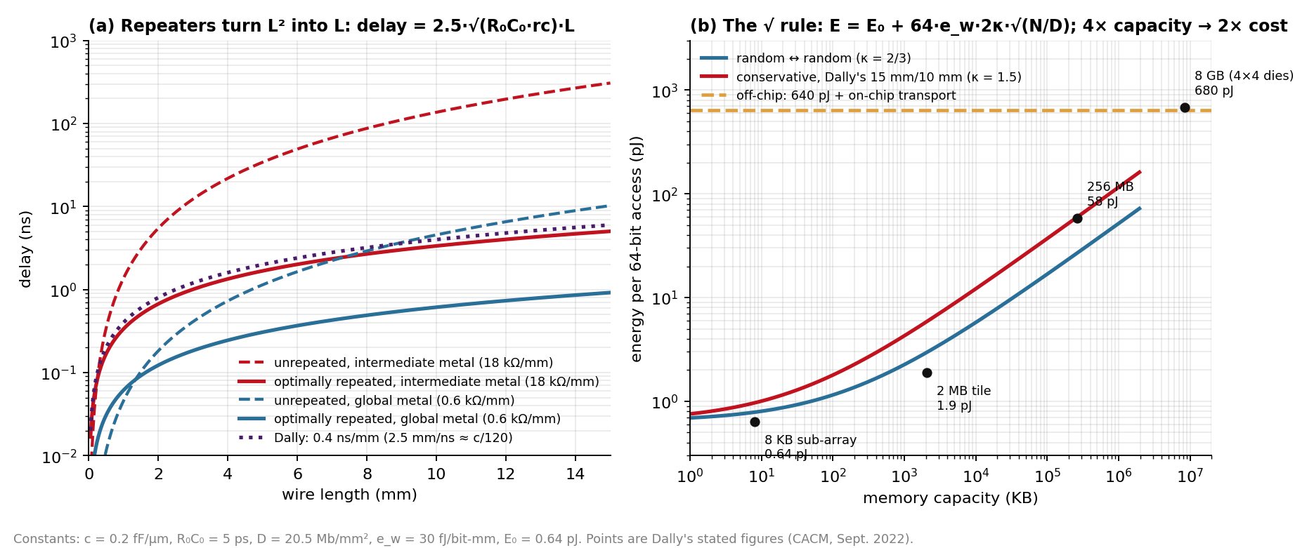
From the 8 KB sub-array to the 256 MB block the capacity grows 32,768× and the transport cost grows √32,768 ≈ 181×. The endpoint cost (0.64 pJ) is fixed, so small memories are endpoint-dominated and large ones are wire-dominated; the crossover is around 32 KB–256 KB, which is, not coincidentally, the size of an L1/L2 cache.
9. The sub-array: 0.64 pJ and 300 ps from the structure
Dally's terminal costs are for an 8 KB (64 Kb) SRAM sub-array, the standard building block of large on-chip memories: 256 wordlines × 256 bit-columns of 6T cells. At a 0.021 µm² cell (≈ 0.21 µm along the wordline × 0.10 µm along the bitline), the array is about 54 µm × 26 µm plus decoders, sense amplifiers and drivers: roughly 60 × 45 µm overall.
Energy budget for a 64-bit read (the wordline activates all 256 columns; 64 are selected through a 4:1 column multiplexer):
| Component | Estimate | Per bit |
|---|---|---|
| Wordline: 54 µm of wire (11 fF) + 512 pass-gate gates (≈ 20 fF), full swing, charge and discharge | 31 fF × 0.75² ≈ 17 fJ | 0.3 fJ |
| Row decoder and wordline driver | ≈ 100 fF switched ≈ 30 fJ | 0.5 fJ |
| Bitlines: 256 pairs, each ≈ 13 fF (26 µm of wire + 256 drain junctions), one side discharges ≈ 100 mV and is restored: C·V·ΔV ≈ 13 fF × 0.75 × 0.1 ≈ 1 fJ each | ≈ 250 fJ | 4 fJ |
| 64 sense amplifiers, full-swing internal nodes ≈ 3 fJ each | ≈ 190 fJ | 3 fJ |
| Column mux, local data lines (~60 µm) and output drivers to the sub-array edge | ≈ 120 fJ | 2 fJ |
| Total | ≈ 0.6 pJ | ≈ 10 fJ |
Dally's 0.64 pJ = 10 fJ/bit. Two-thirds of it is bitlines and sense amplifiers, i.e., short wires being charged; the bit cell's own contribution (the ~40 µA it sinks for ~30 ps) is under 1 fJ. In Dally's words, the time and energy to read or write a single bit cell is negligible; the sub-array cost is the cost of its internal wires. Note that a 64-bit read charges 256 bitlines: the 4:1 overfetch is a cheaper version of the same organizational waste that DRAM's 8-kilobit rows exhibit.
Timing budget:
| Stage | Estimate |
|---|---|
| Clock to wordline (predecode, decode, driver: 5–6 gate delays at FO4 ≈ 12 ps) | 60–80 ps |
| Wordline rise: distributed RC (≈ 1.6 kΩ × 31 fF, Elmore ≈ 0.4·RC ≈ 20 ps) plus driver | ≈ 40 ps |
| Bitline signal development: ΔV = 100 mV on 13 fF at ≈ 40 µA cell current: t = CΔV/I ≈ 33 ps, with offset margin | 50–70 ps |
| Sense amplifier resolution | ≈ 40 ps |
| Column mux, local data line, output driver | 40–60 ps |
| Total | ≈ 250–300 ps |
So 300 ps is about 25 gate delays' worth of decode, three short RC lines, and one small-signal sensing step. It is the fixed t₀ that a pure distance model lacks, and it is the reason the 8 KB access is not 24× cheaper in time than the 2 MB access even though it is 24× shorter.
10. Density: 256 MB in 100 mm²
A 5-nm-class high-density 6T cell of 0.021 µm² gives 47.6 Mb/mm² of raw bit cells. A large memory adds sense amplifiers and decoders per sub-array, drivers and repeaters per bank, redundancy rows and columns, ECC bits, power grid, and the routing channels between macros. Array efficiency for compiled macros is 50–65%; for a large multi-bank memory with its interconnect it is closer to 40–45%. Then
256 MB = 2.15 Gb → 2.15 Gb / (47.6 Mb/mm² × 0.43) ≈ 105 mm²,
Dally's "approximately 100 mm²" (20.5 Mb/mm² effective). His summation example uses 2 MB per 1-mm² tile, 16.8 Mb/mm², leaving ~20% of each tile for a core — the same density with a small processor added.
Density matters for the heuristics only through √D: doubling density shrinks every distance, energy and latency by √2. Since SRAM cell area has been nearly flat since the 5-nm node (0.021 µm² at N5 and N3E, 0.0175 at N2), the distances in Dally's examples will not shrink much either; the only way to make a 256 MB memory "closer" now is to stack it.
11. Off-chip: 640 pJ per 64-bit access
10 pJ per bit is the cost of leaving the die by a board-level link, with everything counted. Its physics is different from the on-chip case:
- Termination. Above a few Gb/s, a board trace is a transmission line and must be terminated in its ~50 Ω characteristic impedance or the signal reflects. A terminated link carries a steady current whether or not bits toggle: a 400–500 mV swing into 50 Ω is ~9 mA per lane, roughly 8 mW at a 0.9 V I/O supply, or 0.3–0.8 pJ/bit at 10–25 Gb/s for the driver current alone.
- Pad and package capacitance. The pad, ESD structure, bump, package trace and via add 0.5–2 pF at each end: thousands of times a gate, and charged at I/O voltages.
- Circuitry. Pre-drivers, equalization (the trace attenuates high frequencies), receiver amplifiers and comparators, clock recovery, PLLs, serializers and deserializers: 1–3 pJ/bit per end in a 5-nm process.
- Protocol. Packetization, CRC, retry buffers, and the on-die wires from the core to the PHY at the die edge (Section 7's 30 fJ/bit-mm over ~5–10 mm ≈ 0.2–0.3 pJ/bit).
Adding both ends: 4–8 pJ/bit for the electrical link plus 1–3 pJ/bit of protocol and on-die transport ≈ 10 pJ/bit, hence 640 pJ per 64-bit transfer. For comparison, contemporary alternatives span more than an order of magnitude: on-package die-to-die links (NVIDIA's ground-referenced signaling, UCIe) ≈ 0.3–1 pJ/bit; HBM ≈ 2–3 pJ/bit; PCIe/Ethernet SerDes ≈ 5–8 pJ/bit; DDR-class DRAM including the DRAM core ≈ 10–20 pJ/bit. Dally's other off-chip figure — 640 pJ to store and later reload a 16-bit activation, i.e., 40 pJ/bit for a write plus a read, 20 pJ/bit per direction — is the DRAM end of that range.
In transport-equivalents, 640 pJ is 333 mm of on-chip wire: crossing a die boundary costs about as much as crossing twenty dies. That single ratio explains the shape of every accelerator built since: keep the working set on the die or on the package, and treat the board as a last resort.
12. Arithmetic, and the constant factors
An add is ~10 fJ. Horowitz's 45-nm, 0.9-V table gives 0.1 pJ for a 32-bit integer add. Between 45 nm and 5 nm the switched capacitance of a small datapath falls roughly 4–5× (gate capacitance and local wire length both scale with pitch) and V² falls 0.9²/0.75² = 1.44×, so 0.1 pJ / (4.5 × 1.44) ≈ 15 fJ; a 16-bit add is about half that. Dally's "64,000×" is 640 pJ / 10 fJ: the off-chip access costs as much as sixty-four thousand additions. A first-principles version: a 32-bit adder is ~1,000 transistors with ~30–50 fF of total switched capacitance at ~30% activity, giving 10–15 fF × 0.56 V² ≈ 6–8 fJ, plus clocking and register overhead.
Why the gap was 15× and is now 64,000×. Dally's aside that a 1.2 nJ memory access was once "only 15×" an add refers to an era when an add cost ~80 pJ (a 1-µm process at 5 V: Horowitz's 0.1 pJ scaled by ~20× in capacitance and 31× in V²). Both halves follow from Section 2: the add's energy fell as C·V² with the transistor — four orders of magnitude — while the memory access's energy is a wire's C·V² plus an I/O budget, and fell only 2×.
The summation example. Local access 1.92 pJ (1 mm round trip); random access 640 + 41 = 681 pJ (Dally rounds to 680). The ratio of communication energies is 681 / 1.92 = 354×, his figure. His "230×" for the whole computation follows if the fixed per-element costs are added to both sides: the sub-array read (0.64 pJ) and the add itself (a 64-bit floating-point add is ~0.3–0.4 pJ at 5 nm): (681 + 0.64 + 0.35) / (1.92 + 0.64 + 0.35) ≈ 234. Dally does not show that decomposition; it is the simplest reading that reproduces the number.
Store or recompute. A 16-bit multiply-accumulate at 5 nm costs ≈ 0.16 pJ (Horowitz's 45-nm FP16 multiply 1.1 pJ + add 0.4 pJ, scaled by ~1/9 for capacitance and voltage, with fusion). Recomputing an activation costs n MACs; storing and reloading it off-chip costs 640 pJ. Recompute wins when n × 0.16 pJ < 640 pJ, i.e., n < 4,000 — Dally's threshold. For a typical MLP layer with n = 256, recomputation costs 41 pJ, sixteen times cheaper than the store. The same arithmetic, with HBM instead of DDR (≈ 3 pJ/bit, ≈ 100 pJ per activation round trip), moves the threshold to n ≈ 600; it is the reasoning behind FlashAttention and every other recompute-instead-of-store kernel.
13. Recipe: regenerate the numbers for any process
Inputs (six constants):
- c — wire capacitance per unit length. Geometry gives 0.15–0.25 fF/µm; use 0.2 unless you know the stack.
- r — wire resistance per unit length for the metal you can afford to route buses on: ρ_eff / (W·H). 5–20 kΩ/mm at 5 nm intermediate metal.
- V — supply voltage of the logic domain (0.65–0.8 V at 5–3 nm; ~1.0 V at 28 nm).
- R₀C₀ — inverter time constant, ≈ FO4/2.5; 4–6 ps at 5 nm, ~10 ps at 28 nm.
- D — effective SRAM density: raw cell density × array efficiency (~0.4–0.6).
- e_io — off-chip energy per bit for the link in question (0.3–20 pJ/bit; see Section 11).
Derived transport constants:
- e_w = α · ½ · c · (1 + f_rep) · V², with activity α (0.5 for random data, 1 for worst case) and repeater overhead f_rep ≈ 0.3.
- v = 1 / (2.5 · √(R₀C₀ · r · c)), then divide by ~1.2–1.5 for pipelining and arbitration on a real fabric.
- L_seg = √(0.7 · R₀C₀ / (0.4 · r·c)) — spacing between repeaters (a sanity check: 30–300 µm).
Terminal (sub-array) costs: E₀ ≈ 10 fJ/bit × b, t₀ ≈ 25 gate delays. Scale E₀ with c·V² and t₀ with FO4 for other processes.
Distances: L = √(N/D); one-way distance κL with κ from the table in Section 8 (½ center, ⅔ random-pair, 1 corner-mean, 1.5 conservative, 2 worst).
Access cost: E = E₀ + b · e_w · 2κL (+ e_io · b if off-chip); t = t₀ + 2κL / v (+ link latency if off-chip).
Python that reproduces the table in Section 0:
import math
# --- process constants (5-nm class, ~2022) ---
c    = 0.2e-15 * 1e3      # F/mm   (0.2 fF/um)
r    = 18e3               # ohm/mm (intermediate metal)
V    = 0.75               # V
R0C0 = 5e-12              # s
D    = 20.5e6 / 8         # bytes/mm^2 (20.5 Mb/mm^2)
e_io = 10e-12             # J/bit, off-chip link
alpha, f_rep = 0.5, 0.3   # activity factor, repeater capacitance overhead
E0, t0 = 0.64e-12, 0.3e-9 # sub-array terminal cost for a 64-bit access

e_w  = alpha * 0.5 * c * (1 + f_rep) * V**2          # J per bit-mm
v    = 1 / (2.5 * math.sqrt(R0C0 * r * c)) / 1.25    # mm/s, incl. pipelining overhead
Lseg = math.sqrt(0.7 * R0C0 / (0.4 * r * c))         # mm between repeaters

def access(kappa, N_bytes=None, L=None, b=64, offchip=False):
    L = L if L is not None else math.sqrt(N_bytes / D)  # side of the square, mm
    d = 2 * kappa * L                                   # round-trip distance, mm
    E = E0 + b * e_w * d + (e_io * b if offchip else 0)
    t = t0 + d / v
    return L, d, E, t

print(f"e_w = {e_w*1e15:.0f} fJ/bit-mm  v = {v*1e-9:.2f} mm/ns (c/{3e11/v:.0f})  L_seg = {Lseg*1e3:.0f} um")
cases = [("8KB sub-array",      dict(kappa=2/3, N_bytes=8*1024)),
         ("2MB tile (center)",  dict(kappa=0.5, N_bytes=2*2**20)),
         ("256MB, random pair", dict(kappa=2/3, N_bytes=256*2**20)),
         ("256MB, Dally 15mm",  dict(kappa=1.5, N_bytes=256*2**20)),
         ("16mm die, random",   dict(kappa=2/3, L=16.0)),
         ("4x4 dies, random",   dict(kappa=2/3, L=16.0, offchip=True))]
for name, kw in cases:
    L, d, E, t = access(**kw)
    print(f"{name:20s} L={L:5.2f} mm  round trip={d:6.2f} mm  E={E*1e12:7.2f} pJ  t={t*1e9:5.2f} ns")
Output with the constants above: e_w ≈ 37 fJ/bit-mm, v ≈ 2.4 mm/ns (c/126), L_seg ≈ 49 µm; the 256 MB "Dally 15 mm" line gives ≈ 72 pJ and 13.2 ns, the 16-mm-die random access ≈ 51 pJ and 9.2 ns, and the off-chip case ≈ 691 pJ. The residual difference from Dally's 58 pJ is the (V, α, repeater) convention of Section 7: setting α·(1 + f_rep) = 0.5 and V = 0.78 V gives e_w = 30.4 fJ and 59 pJ. Everything else in the article follows by substituting the appropriate N, κ and b.
14. Where the heuristics bend
- Activity and swing. The 30 fJ constant assumes random data at full swing. Low-swing or differential on-chip signaling can cut it 2–4×; worst-case patterns with crosstalk can double it. Quote the convention.
- Pipelining and queueing. 0.4 ns/mm is a transport velocity. A network-on-chip adds a cycle or more per router and, under load, queueing that can exceed the wire time. Dally's 12.3 ns is an unloaded figure.
- Which metal. Buses on upper, wider layers are 3–5× faster per millimeter than the intermediate-layer estimate, but there is little of that metal. Velocity is really a budget decision about which wires get the good layers.
- Which statistic. Mean, percentile, or worst-case distance differ by up to 3× for the same memory (Section 8). Latency budgets need a high percentile; energy budgets need the mean.
- Third dimension. Hybrid-bonded stacking replaces √(N/D) with a vertical hop of tens of micrometers. It is the one lever that changes the square-root rule's constant by an order of magnitude; the 2026 generation of stacked caches and HBM base dies is the first large-scale use of it.
- Off-chip variance. e_io spans 0.3–20 pJ/bit across link types. "640 pJ" is a board-level figure; on-package it would be ~20–60 pJ.
- Locality is the whole point. The square-root rule prices uniformly random access. Any locality — sequential runs, tiles, reuse — replaces √N by the size of the working set that actually moves. That is Dally's argument: since the constant factors are 10²–10⁵, an algorithm's placement of data is not a detail but the dominant term in its cost, and a model of computation that cannot express it cannot rank algorithms correctly.
References
- W. J. Dally, "On the Model of Computation: Point — We Must Extend Our Model of Computation to Account for Cost and Location," Communications of the ACM 65(9), pp. 30–32, Sept. 2022. (All quoted figures.)
- W. J. Dally, Y. Turakhia, S. Han, "Domain-Specific Hardware Accelerators," CACM 63(7), 2020.
- H. B. Bakoglu, Circuits, Interconnections, and Packaging for VLSI, Addison-Wesley, 1990. (Optimal repeater insertion: k_opt, h_opt, T_min = 2.5√(R₀C₀RC).)
- W. C. Elmore, "The Transient Response of Damped Linear Networks with Particular Regard to Wideband Amplifiers," J. Applied Physics 19, 1948. (Elmore delay.)
- T. Sakurai, "Closed-Form Expressions for Interconnection Delay, Coupling, and Crosstalk in VLSI's," IEEE Trans. Electron Devices 40(1), 1993.
- R. Ho, K. W. Mai, M. A. Horowitz, "The Future of Wires," Proc. IEEE 89(4), 2001.
- M. Horowitz, "Computing's Energy Problem (and What We Can Do About It)," ISSCC, 2014. (45-nm energy table used for scaling arithmetic costs.)
- W. J. Dally and J. W. Poulton, Digital Systems Engineering, Cambridge University Press, 1998. (Off-chip signaling physics: termination, transmission lines, link budgets.)
- J. W. Poulton et al., "A 1.17-pJ/b, 25-Gb/s/pin Ground-Referenced Single-Ended Serial Link for Off- and On-Package Communication Using a Process- and Temperature-Adaptive Voltage Regulator," IEEE JSSC 54(1), 2019. (On-package link energies.)
- B. Keller et al., "A 17–95.6 TOPS/W Deep Learning Inference Accelerator with Per-Vector Scaled 4-bit Quantization for Transformers in 5nm," VLSI Symposium, 2022. (The 5-nm context of Dally's group's contemporaneous work.)
- TSMC N5 and Intel/TSMC ISSCC 2025 SRAM disclosures as reported (0.021 µm² HD bit cell; ~38 Mb/mm² macro density at N2/18A).
All numbers not attributed to a source are the author's estimates from the formulas given; they are intended to reproduce Dally's figures to within the precision he quotes, not to describe any specific product.